100W aluminum nitride ceramic substrate loading chip with wide solder pad and 50 Ohms impedance

A technology of aluminum nitride ceramics and aluminum nitride substrates, applied in electrical components, circuits, waveguide-type devices, etc., can solve the problems affecting product return loss, convenience of welding, unfavorable welding firmness, burnout, etc.

Inactive Publication Date: 2012-04-25
苏州市新诚氏通讯电子股份有限公司
View PDF4 Cites 0 Cited by
  • Summary
  • Abstract
  • Description
  • Claims
  • Application Information

AI Technical Summary

Problems solved by technology

[0002] The aluminum nitride ceramic substrate load sheet is mainly used to absorb the reverse input power of the communication components in the communication base station. If it cannot withstand the required power, the load will burn out. In the actual use of the aluminum nitride ceramic substrate load sheet , all need to have leads soldered to the pads of the load chip. At present, most of the market adopts the design process of small pads, because the enlarged pads will directly affect the return loss of the product, which will increase the return loss. But if The use of small pads will adversely affect the convenience of welding and the firmness of welding

Method used


Image

  • 100W aluminum nitride ceramic substrate loading chip with wide solder pad and 50 Ohms impedance
  • 100W aluminum nitride ceramic substrate loading chip with wide solder pad and 50 Ohms impedance

Examples


Embodiment Construction

[0011] Preferred embodiments of the present invention will be described in detail below in conjunction with the accompanying drawings.

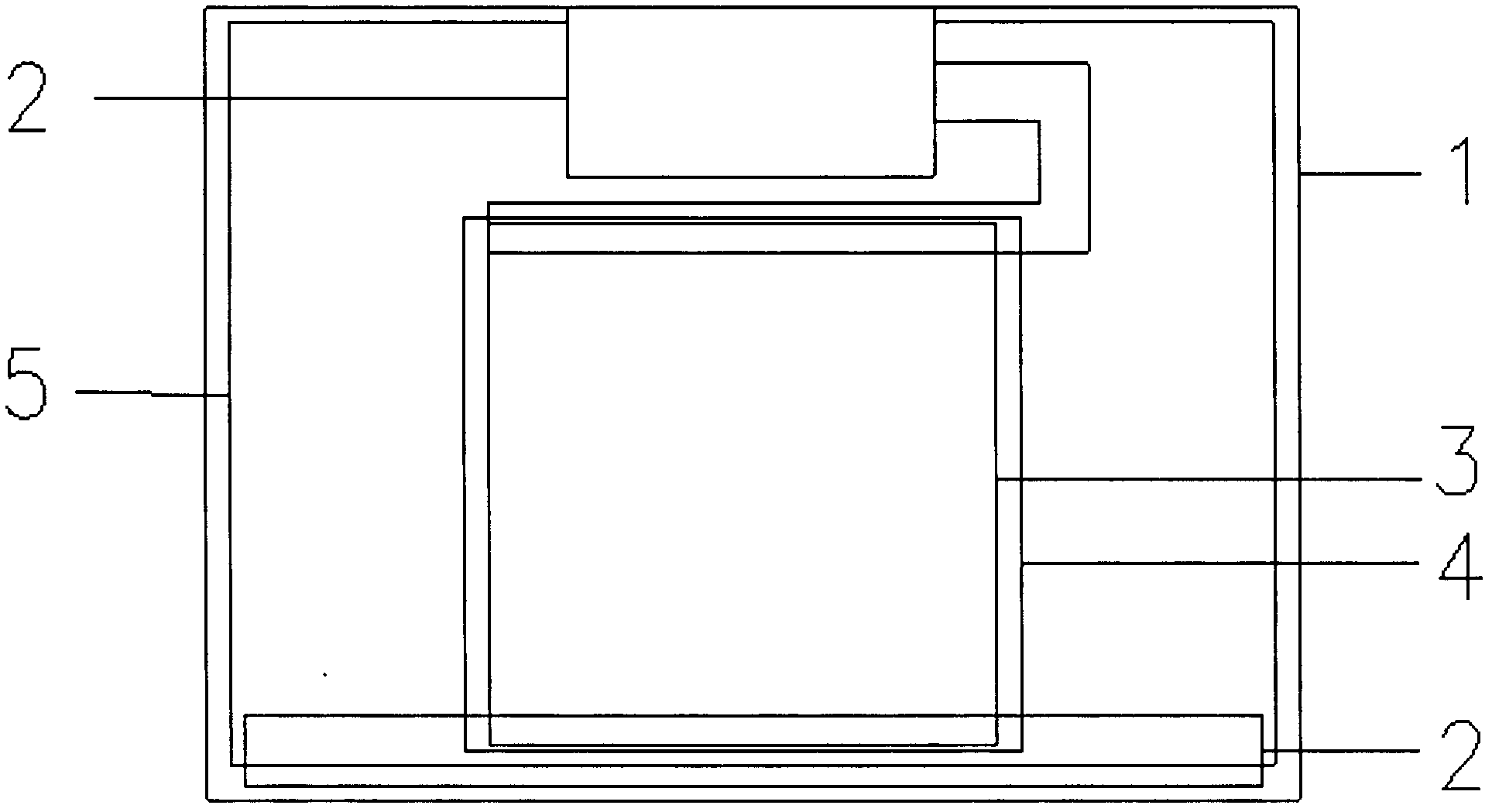
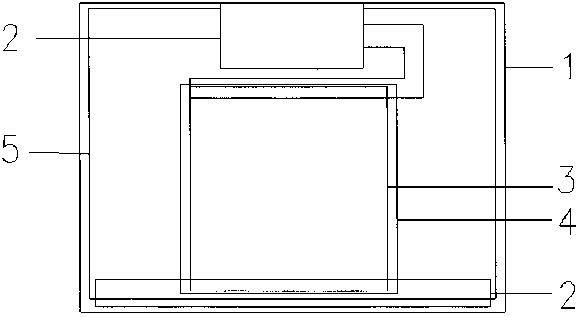
[0012] Such as figure 1 As shown, the wide pad impedance is 50Ω aluminum nitride ceramic substrate 100 watts load chip includes a 5.7*8.9*1.0mm aluminum nitride substrate 1, the back of the aluminum nitride substrate 1 is printed with a back conductive layer, aluminum nitride The front side of the substrate 1 is printed with a resistor 3 and a wire 2. The wire 2 is connected to the resistor 3 to form a load circuit. The ground terminal of the load circuit is electrically connected to the back conductive layer through silver paste, so that the load circuit is grounded and conducted. The back conducting layer and wire 2 are printed with conductive silver paste, and the resistor 3 is printed with resistive paste. A glass protective film 4 is printed on the resistor 3 . A layer of blue protective film 5 is also printed on the upper surfaces of ...


PUM


Abstract

The invention discloses a 100W aluminum nitride ceramic substrate loading chip with a wide solder pad and 50 Ohms impedance, which comprises a 5.7*8.9*1.0mm aluminum nitride substrate, a back conducting layer is printed on the back of the aluminum nitride substrate, a resistor and a wire are printed on the front of the aluminum nitride substrate, the wire is connected with the resistor to form a loading circuit, a grounding end of the loading circuit is electrically connected with the back conducting layer, and a glass protective film is printed on the resistor. The 100W aluminum nitride ceramic substrate loading chip with a wide solder pad and 50 Ohms impedance of the structure has excellent VSWR (Voltage Standing Wave Ratio) performance, power on the 5.7*8.9*1.0mm aluminum nitride ceramic substrate reaches 100W, and meanwhile, the property reaches 3G, so that an aluminum nitride ceramic substrate of the size has wider use range and can be better matched with equipment.

Description

technical field [0001] The invention relates to a loading sheet of an aluminum nitride ceramic substrate, in particular to a 100-watt loading sheet of an aluminum nitride ceramic substrate with a wide pad impedance of 50Ω. Background technique [0002] The aluminum nitride ceramic substrate load sheet is mainly used to absorb the reverse input power of the communication components in the communication base station. If it cannot withstand the required power, the load will burn out. In the actual use of the aluminum nitride ceramic substrate load sheet , all need to have leads soldered to the pads of the load chip. At present, most of the market adopts the design process of small pads, because the enlarged pads will directly affect the return loss of the product, which will increase the return loss. But if The use of small pads will adversely affect the convenience of welding and the firmness of welding. Contents of the invention [0003] In view of the above-mentioned defi...

Claims


Application Information

Patent Timeline
IPC IPC(8): H01P1/22
Inventor 郝敏
Owner 苏州市新诚氏通讯电子股份有限公司
Why Eureka
Try Eureka