Differential reference voltage buffer
A technology of voltage buffer and differential reference, which is applied in the direction of logic circuit connection/interface layout, reliability improvement and modification, etc., and can solve problems affecting the performance and accuracy of data converters, voltage fluctuations, etc.
- Summary
- Abstract
- Description
- Claims
- Application Information
AI Technical Summary
Problems solved by technology
Method used
Image


Examples
Embodiment Construction
[0024] Preferred embodiments of the present invention will be described in detail below in conjunction with the accompanying drawings.
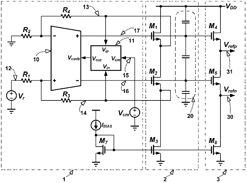
[0025] figure 1 is a schematic circuit diagram of the differential reference voltage buffer of the present invention, such as figure 1 As shown, it includes three parts: a control part 1 , a main buffer part 2 and a copy buffer part 3 , and the main buffer part 2 is connected in series between the control part 1 and the copy buffer part 3 .
[0026] The control part 1 includes a fully differential operational amplifier 10, a common-mode feedback circuit 11 and four resistors R 1 , R 2 , R 3 and R 4 , and R 1 = R 2 , R 3 = R 4 , the output terminal of the common-mode feedback circuit 11 is connected to the common-mode feedback input terminal of the fully differential operational amplifier 10 to determine its output common-mode level.
[0027] Resistance R 1 and R 2 One end is connected to the ground gnd and the reference voltage Vr,...
PUM
 Abstract
Description
Claims
Application Information
 - R&D
- Intellectual Property
- Life Sciences
- Materials
- Tech Scout
- Unparalleled Data Quality
- Higher Quality Content
- 60% Fewer Hallucinations
Browse by: Latest US Patents, China's latest patents, Technical Efficacy Thesaurus, Application Domain, Technology Topic, Popular Technical Reports.
© 2025 PatSnap. All rights reserved.Legal|Privacy policy|Modern Slavery Act Transparency Statement|Sitemap|About US| Contact US: help@patsnap.com