Defect point locating method of semiconductor device

A positioning method and defect point technology, applied in the field of semiconductor device defect point positioning, can solve the problems of complicated installation and debugging, reduce failure analysis efficiency, increase failure analysis cost, etc., and achieve the effect of improving efficiency and reducing cost.

Active Publication Date: 2014-01-22
CSMC TECH FAB2 CO LTD
View PDF5 Cites 0 Cited by
  • Summary
  • Abstract
  • Description
  • Claims
  • Application Information

AI Technical Summary

Problems solved by technology

[0004] Through the research of the existing technology, the inventor found that the cost of the laser marking machine used in the existing technical solution is extremely high, which increases the cost of failure analysis, and the installation and debugging are very complicated, which reduces the efficiency of failure analysis

Method used


Image

  • Defect point locating method of semiconductor device
  • Defect point locating method of semiconductor device
  • Defect point locating method of semiconductor device

Examples


Embodiment 1

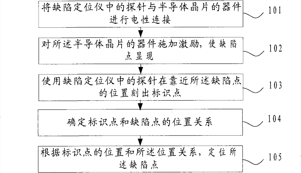
[0051] figure 1 It is a schematic flow chart of a method for locating a defect point of a semiconductor device provided in Embodiment 1 of the present invention. The method specifically may include the following steps:

[0052] Step 101 , electrically connect the probes in the defect locator to the devices of the semiconductor wafer.

[0053] Load the semiconductor wafer into the defect locator, and configure the probes in the defect locator; by adjusting the position angle of the semiconductor wafer on the tray and the position of the probes, the probes at different positions correspond to the devices in the semiconductor wafer. Make physical and electrical contact.

[0054] Step 102, applying excitation to the devices of the semiconductor wafer to make defect points appear.

[0055] Turn on the power signal line to apply excitation to the devices in the semiconductor wafer, so that the defect points appear; when the power signal is turned on, the probe transmits the test ...

Embodiment approach

[0071] One: use the probe to carve a mark point at a position close to the defect point to carve a mark point.

[0072] Two: use the probe to carve out marking points at a position close to the defect point and carve at least two marking points.

[0073] Wherein, using the probe to engrave at least two identification points at a position close to the defect point can be achieved in the following manner:

[0074] Use the probe to carve out a mark point at a position close to the defect point to carve out a mark point;

[0075] moving the probe back to the initial position, and applying excitation to the device in the semiconductor wafer again to make the defect point appear again;

[0076] Using the probe again to engrave a marker point at a position close to the defect point to engrave a second marker point;

[0077] Repeat the above steps to set multiple identification points for a defect point as required.

[0078] Taking the device in the semiconductor wafer as an exampl...

Embodiment 3

[0086] In Embodiment 1, in the step of applying excitation to the device of the semiconductor wafer to make the defect point appear, when at least two defect points appear, the probe in the defect locator is at a position close to the defect point The step of engraving the marking point may specifically include:

[0087] Move the probe in the defect locator to a position close to one of the defect points;

[0088] Mark a marker point at the location using the probe;

[0089] moving the probe back to its initial position;

[0090] Apply excitation to the devices of the semiconductor wafer again to make the defect point appear again;


PUM


Abstract

The invention discloses a defect point locating method of a semiconductor device, which comprises the following steps: a probe in a defect locator is electrically connected with a device of a semiconductor chip; the device of the semiconductor chip is excited so as to enable a defect point to appear; the probe of the defect locator is used to carve an identification point in a position close to the defect point; and the position relationship between the identification point and the defect point is confirmed. According to the method provided by the invention, when the defect point in the device of the semiconductor chip appears due to excitation, the probe of the existing defect locator is used to set the identification point nearby the defect point, so the defect point can be located according to the position of the identification point and the position relationship between the identification point and the defect point. The method has the advantages that an expensive laser marking machine does not need to be adopted, the cost of failure analysis can be reduced, the existing equipment does not need to be refitted at the same time, the failure analysis can be realized conveniently and rapidly, the simplicity and the practicality are achieved, and the efficiency of the failure analysis is improved.

Description

Technical field: [0001] The invention relates to the field of semiconductor manufacturing, in particular to a method for locating defect points of a semiconductor device. Background technique: [0002] With the rapid development of large-scale integrated circuit technology, semiconductor devices have been widely used in aerospace, military, industrial, communication and civilian products. Therefore, it is of great significance to study the reliability of semiconductor devices. Failure analysis is a commonly used method of reliability analysis. It is to obtain the failure mechanism and accurately determine the cause of failure through anatomical analysis of field use failure samples, reliability test failure samples, and screening failure samples, in order to improve product reliability. Provide a scientific basis. [0003] Defect point location is an extremely important step in failure analysis. After the defect point is found and located in the defect locator, the defect ...

Claims


Application Information

Patent Timeline
Patent Type & Authority Patents(China)
IPC IPC(8): G01R31/26
Inventor 周浩
Owner CSMC TECH FAB2 CO LTD
Why Eureka
Try Eureka