Semiconductor fabrication apparatus and temperature adjustment method
A technology for manufacturing equipment and semiconductors, which is applied in the field of semiconductor manufacturing equipment and can solve problems such as difficulty in optimizing flow path design
- Summary
- Abstract
- Description
- Claims
- Application Information
AI Technical Summary
Problems solved by technology
Method used
Image
Examples
Embodiment approach 2
[0081] Figure 6A is a side sectional view of the wafer stage 102 and the water jet 164 according to the second embodiment, Figure 6B It is a plan view of the water injector 164 of Embodiment 2. The semiconductor manufacturing apparatus of Embodiment 2 differs from the semiconductor manufacturing apparatus of Embodiment 1 only in the shape of the cavity 121 of the wafer stage 102 and the structure of the water injector 164 . Therefore, the above differences will be mainly described below.
[0082] The cavity 121 formed in the wafer stage 102 according to Embodiment 2 has a bottom inner wall portion 121a, a peripheral wall portion 121b, and a top inner wall portion 121c. The top inner wall portion 121c and the bottom inner wall portion 121a have inclined surfaces inclined with respect to the mounting surface on which the semiconductor wafer W is mounted. More specifically, the top inner wall portion 121c is formed in an inverted conical shape having an apex below the substan...
Embodiment approach 3
[0093] Figure 8 It is a schematic diagram showing the wafer stage 2 and the temperature control device 306 according to the third embodiment. The semiconductor manufacturing apparatus according to the third embodiment heats and adjusts the temperature of the wafer mounting table 2 by supplying saturated steam into the cavity 21 of the wafer mounting table 2 . The semiconductor manufacturing apparatus according to the third embodiment is different from the first embodiment only in the structure of the wafer mounting table 2 and the temperature control device 306 , and therefore, the above differences will be mainly described below.
[0094] The temperature control device 306 of Embodiment 3 does not include the water injector 64, the temperature controller 62, and the flow sensor 72 described in Embodiment 1, but includes a steam pressure controller 73 for supplying saturated steam into the cavity 21, and Desuperheater 74. In addition, a water vapor supply port (temperature ...
Embodiment approach 4
[0106] Figure 11 It is a schematic diagram showing the wafer stage 2 and the temperature control device 406 according to the fourth embodiment. The wafer semiconductor device according to the fourth embodiment is configured to be capable of heating and cooling the wafer stage 2 by combining the components of the first and third embodiments.
[0107] Like the first embodiment, the wafer stage 2 of the fourth embodiment has a cavity 21 inside, and a water jet 64 is arranged in the cavity 21 . In addition, the wafer stage 2 is provided with the same water vapor supply port 21e as in the third embodiment at an appropriate portion of the bottom inner wall portion 21a.
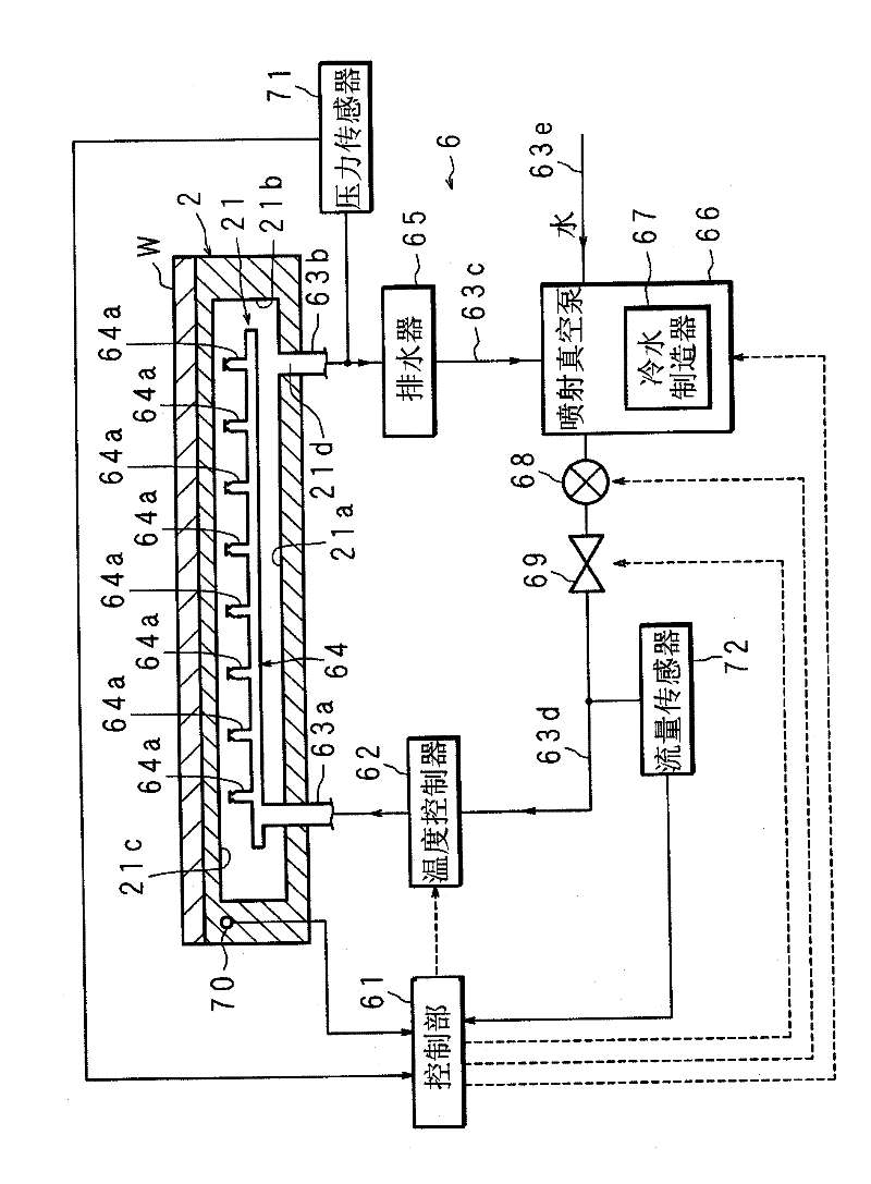
[0108] The temperature adjustment device 406 in Embodiment 4 includes the same control unit 61 as in Embodiment 1, a temperature controller 62, a water injector 64, a drainer 65, a jet vacuum pump 66, a cold water generator 67, a water supply pump 68, and a flow control valve. 69. Temperature sensor 70, pressure ...
PUM
 Abstract
Description
Claims
Application Information
 - R&D
- Intellectual Property
- Life Sciences
- Materials
- Tech Scout
- Unparalleled Data Quality
- Higher Quality Content
- 60% Fewer Hallucinations
Browse by: Latest US Patents, China's latest patents, Technical Efficacy Thesaurus, Application Domain, Technology Topic, Popular Technical Reports.
© 2025 PatSnap. All rights reserved.Legal|Privacy policy|Modern Slavery Act Transparency Statement|Sitemap|About US| Contact US: help@patsnap.com


