
Photoelectric conversion element and method for manufacturing same

A technology for photoelectric conversion elements and manufacturing methods, which is applied to electrical elements, electrical solid-state devices, circuits, etc., can solve problems such as leakage paths, increase dark current, and increase stress, and achieve the effect of suppressing cracks and suppressing the increase of dark current.

Inactive Publication Date: 2012-03-14
SONY SEMICON SOLUTIONS CORP
View PDF6 Cites 7 Cited by
  • Summary
  • Abstract
  • Description
  • Claims
  • Application Information

AI Technical Summary

Problems solved by technology

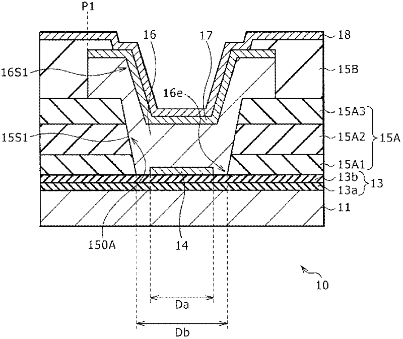
Therefore, stress is applied to the i-type semiconductor layer due to the shape of the hole (the step of the side wall), and cracks are generated.
In particular, if the film thickness of the i-type semiconductor layer is increased in order to enhance optical sensitivity, the stress also becomes large
The problem with this type of crack is that it acts as a leak path and increases dark current

Method used


Image

  • Photoelectric conversion element and method for manufacturing same
  • Photoelectric conversion element and method for manufacturing same
  • Photoelectric conversion element and method for manufacturing same

Examples


Embodiment Construction

[0033] Embodiments of the present invention will be described below with reference to the drawings. Description will be given in the following order.

[0034] 1. Embodiment (Example in which an i-type semiconductor layer is formed within a range from the inside of the contact hole to the upper surface of the first interlayer insulating film)

[0035] 2. Modifications 1 and 2 (example of forming a contact hole by two etching process steps)

[0036] 3. Modifications 3 and 4 (example of patterning i-type semiconductor layer in contact hole)

[0037] 4. Application examples (examples of photoelectric conversion devices and radiation imaging devices using photoelectric conversion elements)

[0038] 1. Example

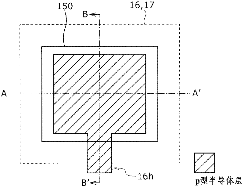
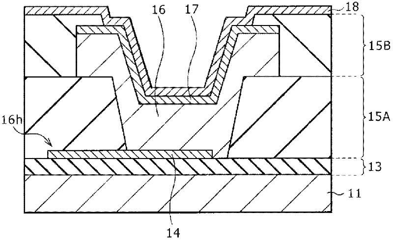
[0039] figure 1 A schematic structure of a photoelectric conversion element 10 according to an embodiment of the present invention is shown. The photoelectric conversion element 10 is a positive-intrinsic-negative (Positive Intrinsic Negative, PIN) photoelectric device ...


PUM


Abstract

The invention relates to a photoelectric conversion element and a method for manufacturing the same. The photoelectric conversion element includes a first semiconductor layer that exhibits a first conductivity type and is provided in a selective area over a substrate, a second semiconductor layer that exhibits a second conductivity type and is disposed opposed to the first semiconductor layer, and a third semiconductor layer that is provided between the first and second semiconductor layers and exhibits a substantially intrinsic conductivity type. The third semiconductor layer has at least one corner part that is not in contact with the first semiconductor layer. The invention can suppress increase in the dark current attributed to the crack or the occurrence itself of the crack.

Description

[0001] Cross References to Related Applications [0002] The present application contains subject matter related to the disclosure of Japanese Priority Patent Application JP 2010-179555 filed in the Japan Patent Office on Aug. 10, 2010, the entire content of which is hereby incorporated by reference. technical field [0003] The present invention relates to a photoelectric conversion element such as a PIN photodiode used in, for example, a radiation imaging apparatus and an optical touch sensor, and a method of manufacturing the same. Background technique [0004] Positive Intrinsic Negative (PIN) photodiodes are used as photoelectric conversion elements in radiation imaging devices, optical touch panels, and the like. This type of PIN photodiode has a structure in which a so-called i-type semiconductor layer is located between a p-type semiconductor layer and an n-type semiconductor layer so that signal charges whose charge amount depends on the light amount of incident lig...

Claims


Application Information

Patent Timeline
Patent Type & Authority Applications(China)
IPC IPC(8): H01L31/105H01L31/0352H01L31/18
CPCH01L27/14607H01L27/14663H01L27/14692H01L31/105H01L31/18H01L31/0352
Inventor 山田泰弘田中勉高德真人伊藤良一
Owner SONY SEMICON SOLUTIONS CORP
Learn More