Method for forming composite functional material structure
A technology of material structure and composite function, applied in the manufacturing of electrical components, circuits, semiconductor/solid-state devices, etc., can solve problems such as strain, fracture, interface difference, etc.
- Summary
- Abstract
- Description
- Claims
- Application Information
AI Technical Summary
Problems solved by technology
Method used
Image

Examples
Embodiment 1
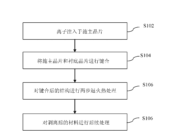
[0042] This embodiment discloses a method for forming a germanium-on-insulator structure by high-energy deep implantation. Figure 2a-Figure 2d It is a schematic diagram of the wafer structure after performing various steps in the method for forming the composite functional material structure in this embodiment. As shown in the figure, this embodiment includes the following steps:
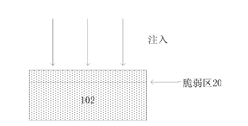
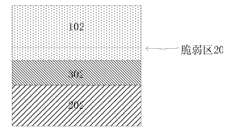
[0043] Step S202: He ion implantation acts on the Ge wafer 102 of the donor wafer, and the dose is 1×10 16 , the energy is 500KeV, the H ion implantation acts on the Ge wafer, and the dose is 3×10 16 cm -2 , the implantation energy is 300KeV, the projected range of H ion and He ion implantation is controlled at 2100nm, and a fragile region 20 is formed around this projected range, such as Figure 2a shown;
[0044] Step S204: growing a layer of SiO on the surface of the substrate wafer Si sheet 202 by thermal oxidation 2 Membrane 302, with a thickness of about 80nm, the Si wafer and the Ge waf...
Embodiment 2
[0048] This embodiment discloses a method for forming LaAlO on insulator 3 The method of thin-layer structure. Figure 3a-Figure 3d It is a schematic diagram of the wafer structure after performing various steps in the method for forming the composite functional material structure in this embodiment. As shown in the figure, this embodiment includes the following steps:
[0049] Step S302: H ion implantation acts on LaAlO 3 Wafer 103 with a dose of 2 x 10 17 cm -2 , the implantation energy is 60KeV, the projected range of ion implantation is controlled at 500nm, and a fragile region 30 is formed around this projected range, such as Figure 3a shown;
[0050] Step S304: LaAlO 3 Wafer 103 and glass (glass) 203 are through cleaning and ion surface activation, two wafers are bonded, as Figure 3b shown;
[0051] Step S306: Perform annealing heat treatment on the bonded structure. The annealing temperature in the first step is 250°C and the annealing time is 40 hours to stre...
Embodiment 3
[0054] This embodiment discloses a method for forming a GaN thin layer structure. Figure 4a-Figure 4d It is a schematic diagram of the wafer structure after performing various steps in the method for forming the composite functional material structure in this embodiment. As shown in the figure, this embodiment includes the following steps:
[0055] Step S402: H ion implantation acts on the donor wafer GaN wafer 104 with a dose of 3×10 17 cm -2 , the energy is 200KeV, the projected range of ion implantation is controlled at 500nm, and a fragile region 40 is formed around this projected range, such as Figure 4a ;
[0056] Step S404: Epitaxially grow a layer of Al on the surface of the donor wafer GaN wafer 104 2 o 3 Film 404, thickness is about 150nm, grows a layer of SiO with a thickness of 200nm by CVD (Chemical Vapor Deposition) on the surface of substrate wafer Si sheet 204 2 Layer 304, after standard cleaning process and ionic surface activation, will undergo Al 2 ...
PUM
| Property | Measurement | Unit |
|---|---|---|
| thickness | aaaaa | aaaaa |
Abstract
Description
Claims
Application Information
 - R&D
- Intellectual Property
- Life Sciences
- Materials
- Tech Scout
- Unparalleled Data Quality
- Higher Quality Content
- 60% Fewer Hallucinations
Browse by: Latest US Patents, China's latest patents, Technical Efficacy Thesaurus, Application Domain, Technology Topic, Popular Technical Reports.
© 2025 PatSnap. All rights reserved.Legal|Privacy policy|Modern Slavery Act Transparency Statement|Sitemap|About US| Contact US: help@patsnap.com