A process for preparing high-efficiency all-back-electrode n-type solar cells by co-diffusion of boron and phosphorus
A technology of full back electrodes and solar cells, applied in the direction of sustainable manufacturing/processing, circuits, electrical components, etc., can solve the problems of cumbersome preparation process, many process influencing factors, and no profit advantage, so as to improve performance and reduce impact Effect
- Summary
- Abstract
- Description
- Claims
- Application Information
AI Technical Summary
Problems solved by technology
Method used
Image
Examples
Embodiment 1
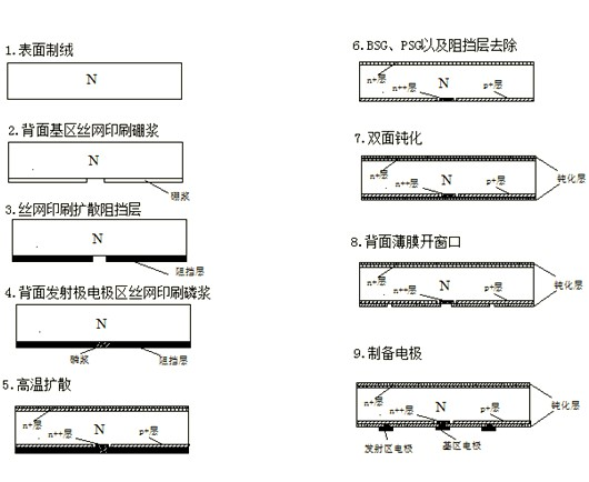
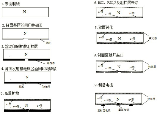
[0022] The front field of the high-efficiency full-back electrode n-type solar cell is a phosphorus-doped structure.
[0023] like figure 1 Shown: a process for preparing high-efficiency full-back electrode n-type solar cells by boron-phosphorus co-diffusion, comprising the following steps:
[0024] 1. Using n-type silicon wafers with a bulk minority carrier lifetime greater than 100μs and a resistivity of 0.5~15.0Ωcm, chemical etching to remove the surface damage layer and texturing;
[0025] 2. Screen printing boron paste in the back emitter area, drying at 100~500℃ for 5~30min;
[0026] 3. Cover the boron paste with another diffusion barrier layer, and dry at 100~500℃ for 5~30min;
[0027] 4. Screen printing the phosphor paste in the contact area of the base area on the back, drying at 100~500℃ for 5~30min;
[0028] 5. Diffusion at high temperature; at 880~1100℃, first diffuse for 10~60min, then cool down to 800~950℃, and then pour POCl 3 source for phosphorus di...
Embodiment 2
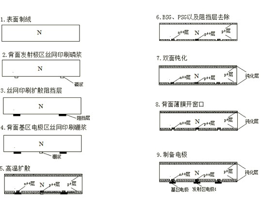
[0034] The front field of the high-efficiency full-back electrode n-type solar cell is a boron-doped suspended junction structure.
[0035] like figure 2 Shown: a process for preparing high-efficiency full-back electrode n-type solar cells by boron-phosphorus co-diffusion, comprising the following steps:
[0036] 1. Using n-type silicon wafers with a bulk minority carrier lifetime greater than 100μs and a resistivity of 0.5~15.0Ωcm, chemical etching to remove the surface damage layer and texturing;
[0037] 2. Screen printing the phosphor paste in the contact area of the base area on the back, drying at 100~500℃ for 5~30min;
[0038] 3. Cover the phosphorous slurry with another diffusion barrier layer, and dry at 100~500℃ for 5~30min;
[0039] 4. Screen printing boron paste in the contact area of the backside emitter, drying at 100~500℃ for 5~30min;
[0040] 5. Diffusion at high temperature, feeding BBr at 880~1100℃ 3 The source is co-diffused with boron and phos...
PUM
 Abstract
Description
Claims
Application Information
 - R&D
- Intellectual Property
- Life Sciences
- Materials
- Tech Scout
- Unparalleled Data Quality
- Higher Quality Content
- 60% Fewer Hallucinations
Browse by: Latest US Patents, China's latest patents, Technical Efficacy Thesaurus, Application Domain, Technology Topic, Popular Technical Reports.
© 2025 PatSnap. All rights reserved.Legal|Privacy policy|Modern Slavery Act Transparency Statement|Sitemap|About US| Contact US: help@patsnap.com


