A kind of igbt device and manufacturing method thereof

A device and doping type technology, applied in semiconductor/solid-state device manufacturing, electrical solid-state devices, semiconductor devices, etc., can solve problems such as substrate cracking, substrate material waste, and substrate area occupation, so as to save manufacturing materials and Process, improve surface area utilization, increase the effect of current density

Inactive Publication Date: 2011-12-14
SUNOVEL SUZHOU TECH
View PDF5 Cites 1 Cited by
  • Summary
  • Abstract
  • Description
  • Claims
  • Application Information

AI Technical Summary

Problems solved by technology

At present, there are attempts to use thin substrates to manufacture IGBTs, but when the thickness of the substrate is less than 180 microns, the substrate is easily cracked during the IGBT device manufacturing process, affecting product yield
Therefore, in the prior art, the substrate and the devices on it are usually formed first, and then the substrate is thinned from the back to manufacture IGBT devices with thinner substrates. However, the IGBT devices formed by this method will cause the substrate The waste of bottom materials reduces production efficiency and material utilization
In another existing IGBT device, such as Figure 1B As shown, in order to form the gate of the MOS transistor, a groove for accommodating the gate is usually formed in the substrate. However, the groove will occupy part of the substrate area, resulting in failure to maximize the current density per unit area in the device.

Method used


Image

  • A kind of igbt device and manufacturing method thereof
  • A kind of igbt device and manufacturing method thereof
  • A kind of igbt device and manufacturing method thereof

Examples


Embodiment Construction

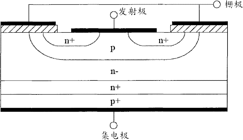
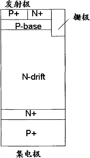
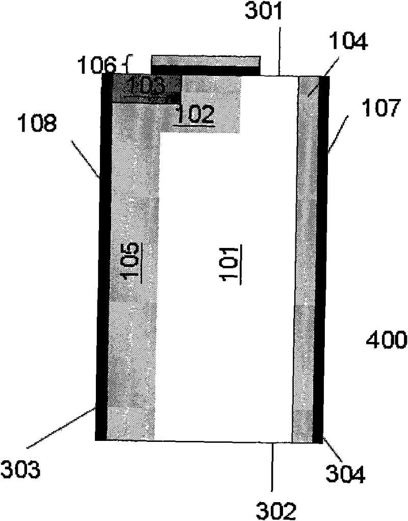
[0013] The following describes in detail the embodiments of the present invention, examples of which are illustrated in the accompanying drawings, wherein the same or similar reference numerals refer to the same or similar elements or elements having the same or similar functions throughout. The embodiments described below with reference to the accompanying drawings are exemplary and are only used to explain the present invention, but not to be construed as a limitation of the present invention. The following disclosure provides many different embodiments or examples for implementing different structures of the invention. In order to simplify the disclosure of the present invention, the components and arrangements of specific examples are described below. Of course, they are only examples and are not intended to limit the invention. Furthermore, the present invention may repeat reference numerals and / or letters in different instances. This repetition is for the purpose of si...


PUM


Abstract

The invention discloses an IGBT (insulated-gate bipolar transistor) device which comprises a substrate, gate regions, a collector electrode contact layer and an emitter contact layer, wherein a duplex diode device and at least one MOS (metal oxide semiconductor) pipe device are formed; the substrate is provided with a first surface, a second surface which is opposite to the first surface, a third surface and a fourth surface which is opposite to the third surface; the gate regions of at least one MOS device are respectively formed on the first surface, the second surface and at least one of the first surface and the second surface; and the collector electrode contact layer and the emitter contact layer of the IGBT device are respectively formed on the third surface and the fourth surface. According to the invention, each contact electrode of the IGBT device are formed by utilizing each surface of an underlayer, and the current intensity of the device is improved; and correspondingly, the invention also discloses a manufacturing method of the IGBT device, the thickness of the underlayer can be effectively utilized by the method, the surface area utilization ratio of the underlayer is improved, thus a thinner IGBT device can be manufactured without introducing the step of reducing the thickness of the underlayer additionally.

Description

technical field [0001] The invention relates to the field of semiconductor manufacturing, in particular to an IGBT device and a manufacturing method thereof. Background technique [0002] In recent years, with the rapid development of the semiconductor industry, the application of power device IGBT (Insulated-gate bipolar transistor) has become more and more extensive. IGBT is not only used in switching circuits, but also widely used in amplifier circuits, frequency conversion and speed regulation. IGBT devices are generally composed of a bipolar transistor and a transistor (MOS tube), such as Figure 1A , shown in B. In order to manufacture IGBT devices with better performance, its substrate thickness is usually required to be less than 200 microns, or even to 80 microns. At present, there are attempts to use thin substrates to manufacture IGBTs, but when the thickness of the substrates is less than 180 microns, the substrates are easily broken during the manufacturing pro...

Claims


Application Information

Patent Timeline
Patent Type & Authority Applications(China)
IPC IPC(8): H01L29/739H01L27/04H01L29/41H01L21/331H01L21/77
Inventor 尹海洲骆志炯朱慧珑
Owner SUNOVEL SUZHOU TECH
Why Eureka
Try Eureka