Optical system wave aberration calibration apparatus and calibration method of using apparatus to test error
A technology of an optical system and a calibration device, applied in the field of optical measurement, can solve the problems of inability to evaluate the test error detection accuracy requirements, test errors, etc.
- Summary
- Abstract
- Description
- Claims
- Application Information
AI Technical Summary
Problems solved by technology
Method used
Image
Examples
specific Embodiment approach 1
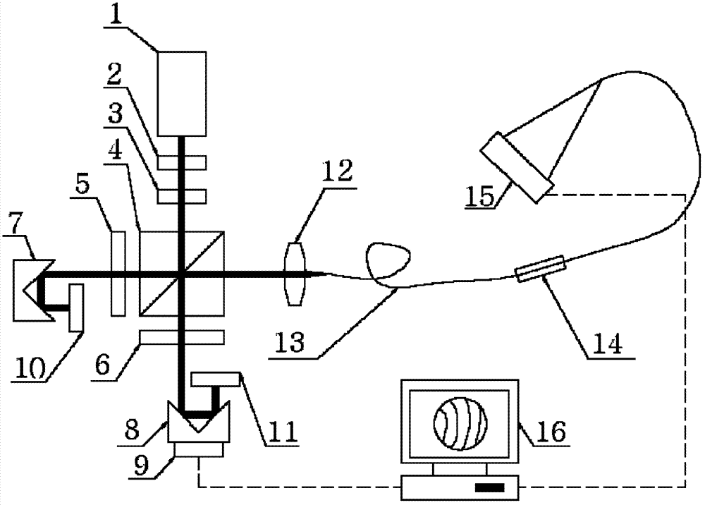
[0023] Specific implementation mode 1. Combination figure 1 Describe the present embodiment, optical system wave aberration calibrating device, this device comprises spectroscopic system, coupling lens 12, reference optical fiber 13, motorized polarization controller 14, photodetector 15, computer 16; It is characterized in that, described spectroscopic system comprises Laser 1, neutral density filter 2, half-wave plate 3, polarization beam splitter prism 4, first quarter-wave plate 5, second quarter-wave plate 6, first corner cube prism 7 , the second corner cube prism 8, the first plane reflector 10 and the second plane reflector 11; the light beam emitted by the laser 1 passes through the neutral density filter 2, the half-wave plate 3 and the polarization beam splitter prism 4 After that, be divided into two beams of orthogonal linearly polarized light, the first beam of linearly polarized light passes through the first quarter-wave plate 5 and the first corner cube prism ...
specific Embodiment approach 2
[0027] Specific embodiment two, the calibration method of the test error of the optical system wave aberration calibration device, the method is completed by the following steps:
[0028] Step 1. Two beams of orthogonal linearly polarized light with a common optical path emitted by the beam splitting system are emitted by the polarization beam splitter prism 4 and then coupled into the reference fiber through the coupling lens 12. The two spherical waves diffracted by the reference fiber 13 interfere to obtain an interference pattern ;
[0029] Step 2. The interferogram obtained in step 1 is collected by the photodetector 15 and then sent to the computer 16, and the piezoelectric ceramic 9 is used for phase shifting. The photoelectric detector 15 collects multiple interferograms; using thirteen steps of phase shifting Algorithms for data processing and analysis to obtain test errors;
[0030] The thirteen-step phase-shifting algorithm is:
[0031] φ = ...
PUM
 Abstract
Description
Claims
Application Information
 - R&D
- Intellectual Property
- Life Sciences
- Materials
- Tech Scout
- Unparalleled Data Quality
- Higher Quality Content
- 60% Fewer Hallucinations
Browse by: Latest US Patents, China's latest patents, Technical Efficacy Thesaurus, Application Domain, Technology Topic, Popular Technical Reports.
© 2025 PatSnap. All rights reserved.Legal|Privacy policy|Modern Slavery Act Transparency Statement|Sitemap|About US| Contact US: help@patsnap.com


