
Graphene memory cell and fabrication methods thereof

A storage unit, graphene technology, applied in the direction of information storage, static memory, digital memory information, etc., can solve the problems of unclear scalability of FeRAM, destructive reading process, etc., to avoid rewriting process, high reliability , The effect of reducing the power used

Inactive Publication Date: 2011-11-23
NAT UNIV OF SINGAPORE
View PDF1 Cites 25 Cited by
  • Summary
  • Abstract
  • Description
  • Claims
  • Application Information

AI Technical Summary

Problems solved by technology

However, the main disadvantage of FeRAM is that the reading process of the "1" state is destructive and requires a subsequent re-writing process to restore the state to "1"
Also, the scalability of FeRAM is still unclear

Method used


Image

  • Graphene memory cell and fabrication methods thereof
  • Graphene memory cell and fabrication methods thereof
  • Graphene memory cell and fabrication methods thereof

Examples


Embodiment Construction

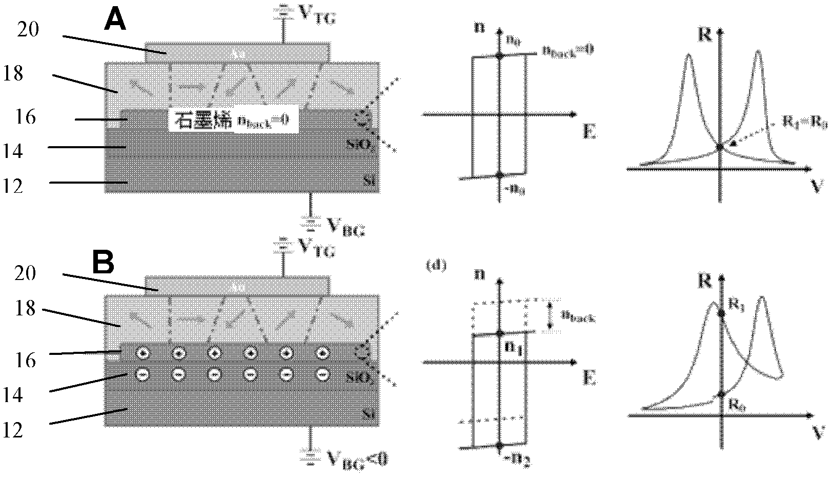
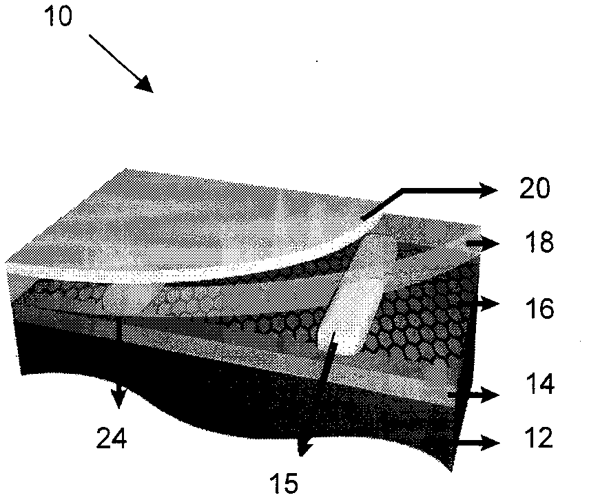
[0044] see Figure 1A and 1B , wherein a preferred embodiment of memory cell 10 is shown. The memory cell 10 includes a conductive substrate 12 and a dielectric layer 14 disposed on the conductive substrate 12 . A graphene layer 16 comprising graphene sheets is disposed on the dielectric layer 14 and encapsulated by a ferroelectric layer 18 comprising a ferroelectric thin film. The graphene layer 16 is electrically connected to the source region 15 and the drain region 17 of the memory unit 10 . The upper electrode 20 electrically connected to the ferroelectric layer 18 and the lower electrode 22 electrically connected to the dielectric layer form two replacement gate regions of the memory cell 10 . Contacts 24 are provided on the graphene layer 16 to connect to / from the memory cell 10 . This arrangement of the above layers forms a non-volatile memory cell with a sandwich structure of metal / ferroelectric / graphene, which in Figure 1B best represented in .

[0045] The gra...


PUM


Abstract

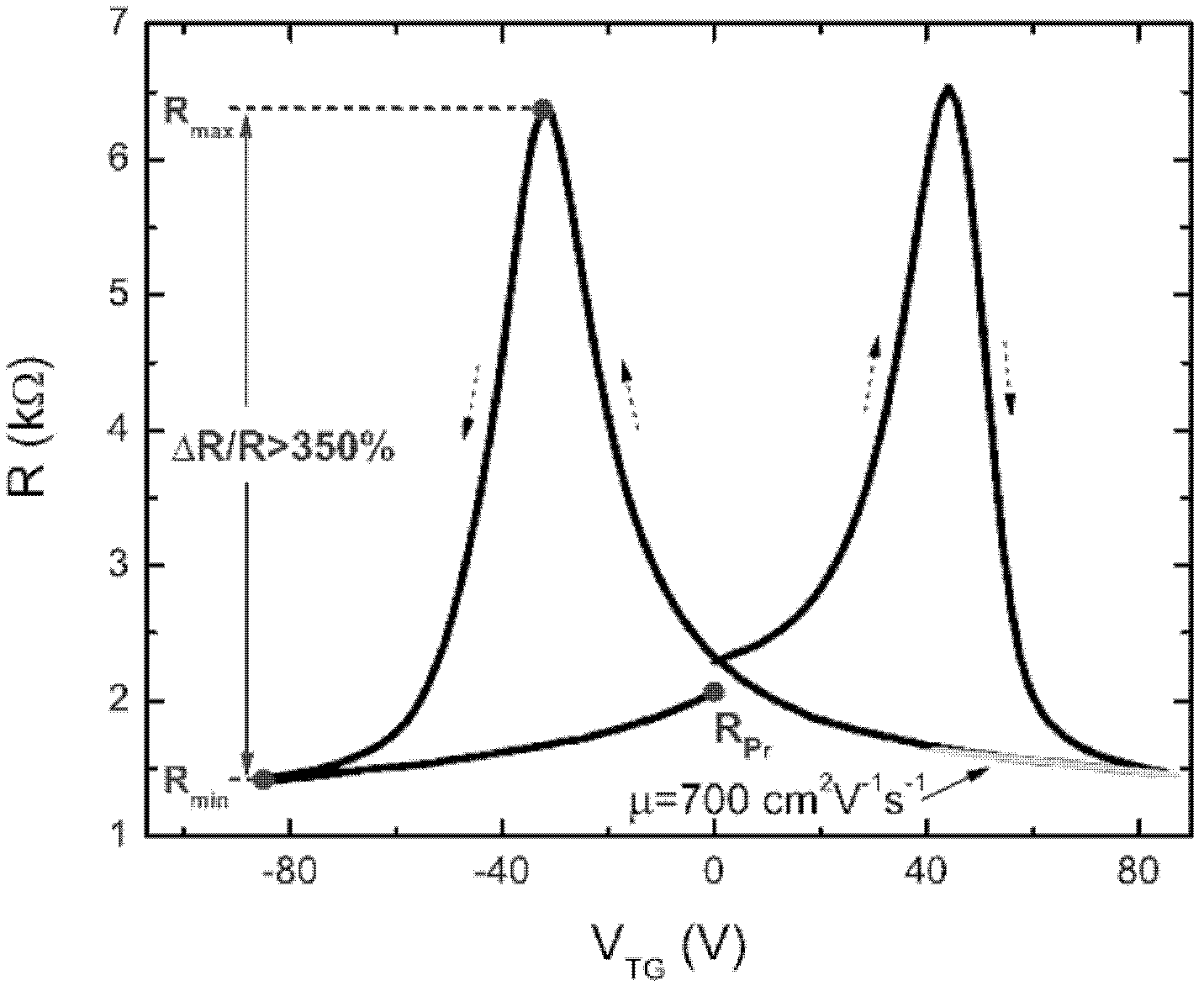
The disclosed memory cell (10) comprises a graphene layer (16) having controllable resistance states representing data values of the memory cell (10). In one exemplary embodiment a non-volatile memory is provided by having a ferroelectric layer (18) control the resistance states. In the exemplary embodiment, binary '0's and ' 1 ' are respectively represented by low and high resistance states of the graphene layer (16), and these states are switched in a non-volatile manner by the polarization directions of the ferroelectric layer (18).

Description

technical field [0001] The present invention generally relates to a memory cell and a method of manufacturing the memory cell. More specifically, the present invention relates, but not exclusively, to a graphene-based memory cell and a method of manufacturing the same. Background technique [0002] For high-performance digital cameras, mp3 players, flash drives and flash memory cards, mobile phones, personal digital assistants (PDAs) and ultra- For portable notebook personal computers (PCs), there is a large demand for memory, and in particular non-volatile memory. [0003] One example of non-volatile memory is NAND flash memory. Essentially, each memory cell of NAND flash memory includes a silicon metal oxide semiconductor field effect transistor (SiMOSFET) with an extra gate, called a floating gate, in addition to a control gate. The floating gate is surrounded by an insulating layer that traps any charges inserted into the floating gate by hot electron tunneling. The ...

Claims


Application Information

Patent Timeline
Patent Type & Authority Applications(China)
IPC IPC(8): H01L21/8236G11C14/00G11C15/04
CPCG11C11/5664H01L29/7781G11C11/5657H01L29/78684G11C13/0014H01L29/784B82Y10/00H01L29/78391H01L29/1606G11C2213/35H01L29/6684G11C11/22G11C13/025
Inventor 巴巴罗斯·欧伊尔迈兹郑毅倪广信杜志达
Owner NAT UNIV OF SINGAPORE
Learn More