Manufacturing method of super-junction semiconductor device

A manufacturing method and semiconductor technology, applied in semiconductor/solid-state device manufacturing, semiconductor devices, electrical components, etc., can solve the problems of reduced withstand voltage reliability and withstand voltage, and achieve the effect of preventing the drop in the withstand voltage qualified product rate

Inactive Publication Date: 2011-09-21
FUJI ELECTRIC CO LTD
View PDF10 Cites 7 Cited by
  • Summary
  • Abstract
  • Description
  • Claims
  • Application Information

AI Technical Summary

Problems solved by technology

That is, even if the designed initial withstand voltage is ensured, in an element having no charge resistance or a small charge resistance in the insulating film 8, the influence of the external charge induced in the insulating film 8 will be lost over time. , the distribution of the electric field on the surface of the substrate changes to generate a concentrated electric field, the withstand voltage gradually decreases, and the reliability of the withstand voltage decreases.

Method used


Image

  • Manufacturing method of super-junction semiconductor device
  • Manufacturing method of super-junction semiconductor device
  • Manufacturing method of super-junction semiconductor device

Examples


Embodiment 1

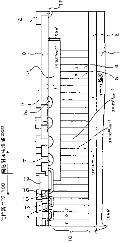
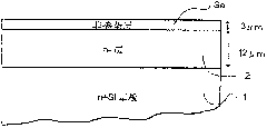
[0061] In Example 1, a method of manufacturing a super junction MOSFET will be described. Figure 3 ~ Figure 12 is expressed in order figure 1 , 2 A cross-sectional view of the main part of the manufacturing process of the super junction semiconductor device (super junction MOSFET) shown. Such as image 3 As shown, at high concentrations n + Si substrate 1 is grown by low-doping epitaxy, for example, 3×10 is formed with a thickness of about 12 μm 14 cm -3 low concentration n - Layer 2, on which an undoped n-layer 3a is formed by epitaxial growth, for example, to a thickness of 3 μm. On the surface of the non-doped n-layer 3a, alignment marks (alignment marks, not shown) required for correct overlapping of each stage of the multi-stage epitaxial layer in the subsequent process are formed.

[0062] Such as Figure 4 As shown, on the above-mentioned non-doped n-layer 3a, an n-type impurity such as phosphorus is ion-implanted 4a on the entire surface at the depth indicate...

Embodiment 2

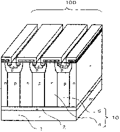
[0069] In embodiment 2, for having in n + Si substrate 1 and low concentration n - The superstructure structure 10 in which n-type and p-type columns are alternately arranged on the layer 2 has n - A super-junction semiconductor device with a low-concentration epitaxial layer 3 illustrates a manufacturing method different from that of Embodiment 1.

[0070] Figure 3 ~ Figure 12 is expressed in order figure 1 , figure 2 A cross-sectional schematic view of the manufacturing process of the super junction semiconductor device (super junction MOSFET) shown. In the same manner as in Example 1, a super junction MOSFET was fabricated. The difference from the manufacturing method of the super junction MOSFET in Example 1 is that in Example 2, in n - When growing the low-concentration epitaxial layers 3e, 3f, and 3g, the hydrogen annealing temperature and the low-doped epitaxial growth start temperature are lower than 1100°C. However, once the epitaxial growth starts, since the...


PUM


Abstract

The present invention provides a manufacturing method of a super-junction semiconductor device. The task of the invention is to provide the manufacturing method of the super-junction semiconductor device, which has the following advantages: capability of preventing impurity concentration variation in forming of a low-concentration first conductive epitaxial layer in a peripheral voltage-resisting structure part or impurity concentration nonuniformity caused by self-doping, and capability of preventing voltage resistance reduction. According to the manufacturing method of the super-junction semiconductor device, in the super-junction structure which is formed by a first conductive area (4) and a second conductive area (5) that constitute a drift layer of the super-junction semiconductor device, a first conductive type doped gas is introduced into an epitaxial growth pipe before a semiconductor source gas when the first conductive area (4) is formed through epitaxial growth.

Description

technical field [0001] The present invention relates to a super-junction structure in which a plurality of arranged n-type columns and p-type columns are adjacent to each other in a direction parallel to the main surface in a direction perpendicular to the main surface of a semiconductor substrate. A method for manufacturing a super junction semiconductor device in which the part is used as a drift layer. Background technique [0002] Generally, semiconductor devices (hereinafter sometimes referred to as semiconductor elements or simply elements) are broadly classified into horizontal elements having electrodes on one surface of a semiconductor substrate and vertical elements having electrodes on both surfaces of a semiconductor substrate . The direction in which the drift current flows when the vertical semiconductor device is turned on is the same as the direction in which the depletion layer extended by the reverse bias voltage (reverse bias voltage) is extended when it ...

Claims


Application Information

Patent Timeline
Patent Type & Authority Applications(China)
IPC IPC(8): H01L21/336H01L21/205H01L29/78
CPCH01L29/1095H01L29/7811H01L29/0634
Inventor 矢嶋理子
Owner FUJI ELECTRIC CO LTD
Why Eureka
Try Eureka