Method for processing blind buried hole on multilayer circuit board
A technology of multi-layer circuit boards and blind buried holes, which is applied in the direction of electrical connection formation of printed components, can solve the problems of high control and electroplating requirements, the yield rate of finished products is less than 80%, and difficult wiring, so as to overcome the phenomenon of board warping , Improve product quality and reduce production costs
- Summary
- Abstract
- Description
- Claims
- Application Information
AI Technical Summary
Problems solved by technology
Method used
Image
Examples
Embodiment 1
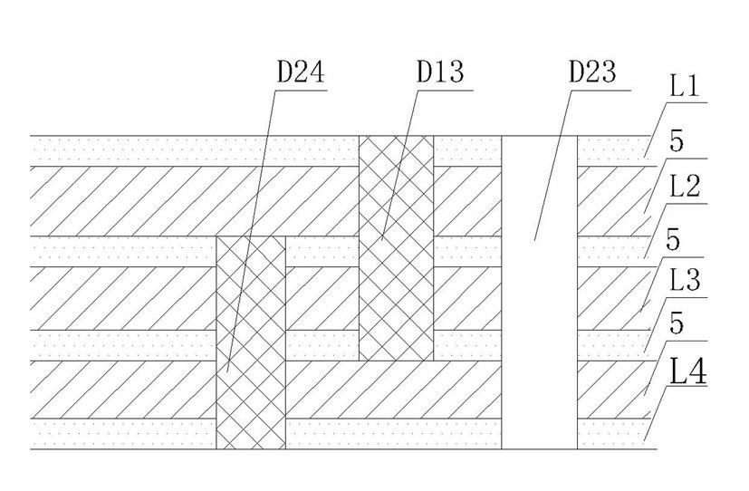
[0027] Such as Figure 4 As shown, the layers of a 4-layer circuit board are: top layer L1, second layer L2, third layer L3, and bottom layer L4. There is a dielectric layer 5 between each layer, and the thickness of the dielectric layer 5 is 0.08mm. Open a 0.25mm mechanical buried hole la in the second layer L2 and the third layer L3, then use a resin plug to bury the hole 1a, and then grind the plate surface with residual resin, electroplate again, make the core board layer circuit, and press it as a whole, and finally in the top layer L1 Open 0.15mm laser blind hole 1b, open 0.15mm laser blind hole 1b on the bottom layer L4, the top layer L1 laser blind hole 1b is electroplated with the mechanical buried hole la of the second layer L2 to form a pad connection, and the bottom layer L4 laser blind hole 1b is connected to the third The mechanical buried hole la of layer L3 is electroplated to form pad connection, and the last four-layer circuit board is drilled through hole 1c...
Embodiment 2
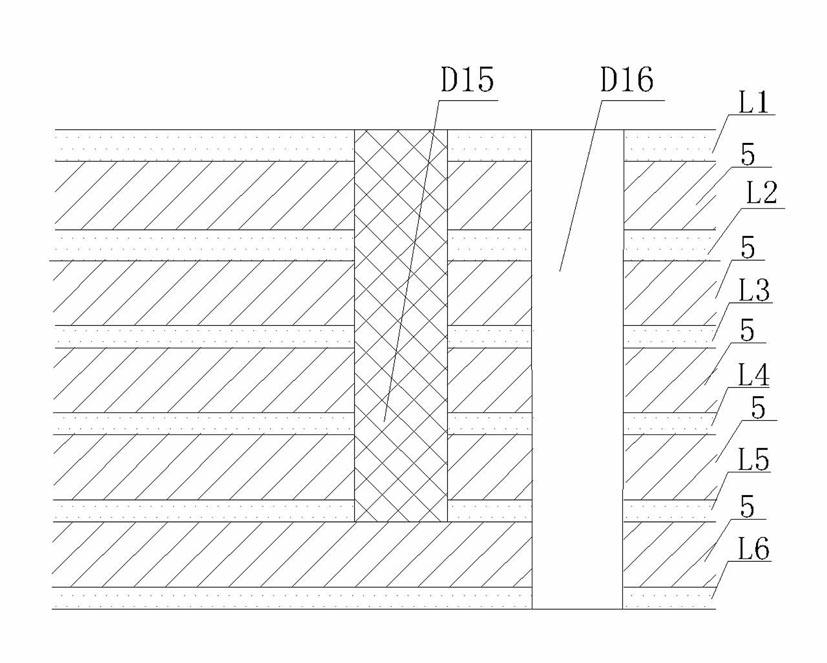
[0029] Such as Figure 5 As shown, the layers of a 6-layer circuit board are: top layer L1, second layer L2, third layer L3, fourth layer L4, fifth layer L5, bottom layer L6, with a dielectric layer 5 between each layer, The thickness of the dielectric layer 5 is 0.08 mm, and a 0.25 mm mechanical buried hole 1a is opened in the second layer L2 to the fifth layer L5, and then the hole 1a is buried with a resin plug, and then the remaining resin is ground on the flat surface, and the core layer is made by electroplating again The circuit is pressed together as a whole, and finally a 0.15mm laser blind hole 1b is opened on the top layer L1. The laser blind hole 1b of the top layer L1 is electroplated with the mechanical buried hole la of the second layer L2 to form a pad connection, and finally the six-layer circuit board is drilled as a whole. 1c.
Embodiment 3
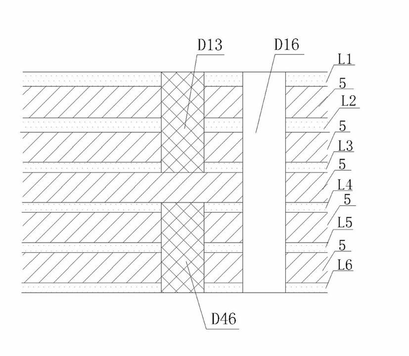
[0031] Such as Figure 6 As shown, the layers of a 6-layer circuit board are: top layer L1, second layer L2, third layer L3, fourth layer L4, fifth layer L5, bottom layer L6, with a dielectric layer 5 between each layer, The thickness of the interlayer dielectric layer 5 is 0.08mm. Laser buried holes la are drilled from the second layer L2 to the third layer L3, and laser blind holes la are drilled from the fourth layer L4 to the fifth layer L5. The aperture size of the laser blind holes is 0.1mm , and then use the electroplating filling process to fill the laser blind hole la, then grind the copper particles and burrs protruding from the flat surface, make the core layer circuit, and press it as a whole. Finally, open a 0.15mm laser blind hole 1b on the top layer L1, and open the bottom layer L6 0.15mm laser blind hole 1b, the top layer L1 laser blind hole 1b and the laser buried hole la of the second layer L2 are filled and electroplated to form a pad connection, and the bot...
PUM
 Abstract
Description
Claims
Application Information
 - Generate Ideas
- Intellectual Property
- Life Sciences
- Materials
- Tech Scout
- Unparalleled Data Quality
- Higher Quality Content
- 60% Fewer Hallucinations
Browse by: Latest US Patents, China's latest patents, Technical Efficacy Thesaurus, Application Domain, Technology Topic, Popular Technical Reports.
© 2025 PatSnap. All rights reserved.Legal|Privacy policy|Modern Slavery Act Transparency Statement|Sitemap|About US| Contact US: help@patsnap.com


