Method for growing phosphorus-silicon-cadmium single crystal
A growth method and cadmium phosphorus technology, applied in the directions of single crystal growth, single crystal growth, crystal growth, etc., can solve the problems of serious vapor convection above the melt, difficult control of flat interface growth, and difficulty in spontaneous nucleation growth. Ensuring single crystal yield, inhibiting vapor convection and fusible melt convection
- Summary
- Abstract
- Description
- Claims
- Application Information
AI Technical Summary
Problems solved by technology
Method used
Image
Examples
Embodiment 1
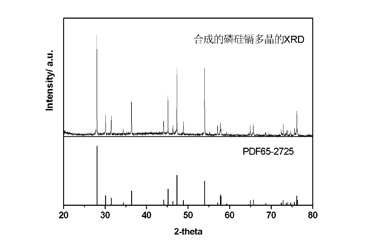
[0033] Embodiment 1, single temperature zone synthesis of cadmium phosphorus silicon polycrystalline material and single crystal growth of cadmium phosphorus silicon cadmium, the steps are as follows:
[0034] 1. Preparation of cadmium phosphorus silicon polycrystalline material
[0035] Put three elemental elements with a purity of 99.999% into a graphite crucible at a ratio of silicon: cadmium: phosphorus = 1:1:2, put the graphite crucible into a quartz tube, and evacuate to 2×10 -4 Seal the quartz tube after Pa. Put the quartz tube into a vertical tubular resistance furnace, raise the temperature of the resistance furnace from room temperature to 350°C at a rate of 30°C / h, and keep it at 350°C for 10-30h. Then the temperature was raised from 350°C to 1150°C at a heating rate of 10°C / h, kept at 1150°C for 20 hours, and then lowered to room temperature. Open the quartz tube, and what is obtained in the graphite crucible is the polycrystalline material of phosphorus, silicon...
Embodiment 2
[0039] Embodiment 2, single-temperature-zone synthesis of cadmium-phosphorus-silicon polycrystalline material and growth of cadmium-phosphorus-silicon single crystal, the steps are as follows:
[0040] 1, the synthesis of phosphorus-silicon-cadmium polycrystalline material, as described in embodiment 1 step 1, the difference is: in the synthesis of phosphorus-silicon-cadmium polycrystalline material, three kinds of elemental elements are by silicon: cadmium: phosphorus=1: 1: The ratio of 2.02 is packed in the graphite crucible, and other steps and parameters are all the same as in Example 1.
[0041] 2. Phosphorous silicon cadmium single crystal growth
[0042] Put the cadmium phosphorus silicon seed crystal into the seed bag of the boron nitride growth crucible, then put the cadmium phosphorus silicon polycrystalline material synthesized in step 1 into the boron nitride growth crucible, and put the boron nitride growth crucible into In the quartz tube, evacuate to 2×10 -4 A...
Embodiment 3
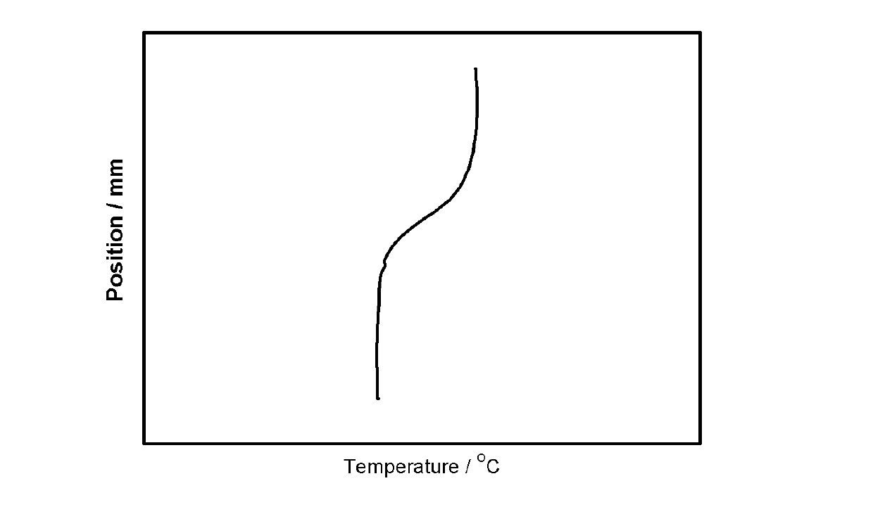
[0043] Embodiment 3, as described in Example 1, the difference is: in step 2, the temperature in the high temperature zone is kept at 1160°C, the temperature gradient in the gradient zone is at 8°C / cm, and the temperature in the low temperature zone is kept at 1090°C; After 30 hours of heat preservation in the high temperature zone, the crucible was lowered.
PUM
| Property | Measurement | Unit |
|---|---|---|
| band gap | aaaaa | aaaaa |
| melting point | aaaaa | aaaaa |
Abstract
Description
Claims
Application Information
 - R&D Engineer
- R&D Manager
- IP Professional
- Industry Leading Data Capabilities
- Powerful AI technology
- Patent DNA Extraction
Browse by: Latest US Patents, China's latest patents, Technical Efficacy Thesaurus, Application Domain, Technology Topic, Popular Technical Reports.
© 2024 PatSnap. All rights reserved.Legal|Privacy policy|Modern Slavery Act Transparency Statement|Sitemap|About US| Contact US: help@patsnap.com


