
Electrostatic protection structure

A technology of electrostatic protection and resistance, applied in circuits, electrical components, electrical solid devices, etc., can solve the problems of occupying chip area and increasing chip cost.

Inactive Publication Date: 2011-08-17
SUZHOU HUAXIN MICROELECTRONICS
View PDF3 Cites 5 Cited by
  • Summary
  • Abstract
  • Description
  • Claims
  • Application Information

AI Technical Summary

Problems solved by technology

Since this structure needs to withstand a large current during ESD, it generally occupies a large proportion of the chip area, resulting in an increase in chip cost

Method used


Image

  • Electrostatic protection structure
  • Electrostatic protection structure
  • Electrostatic protection structure

Examples


Embodiment 1

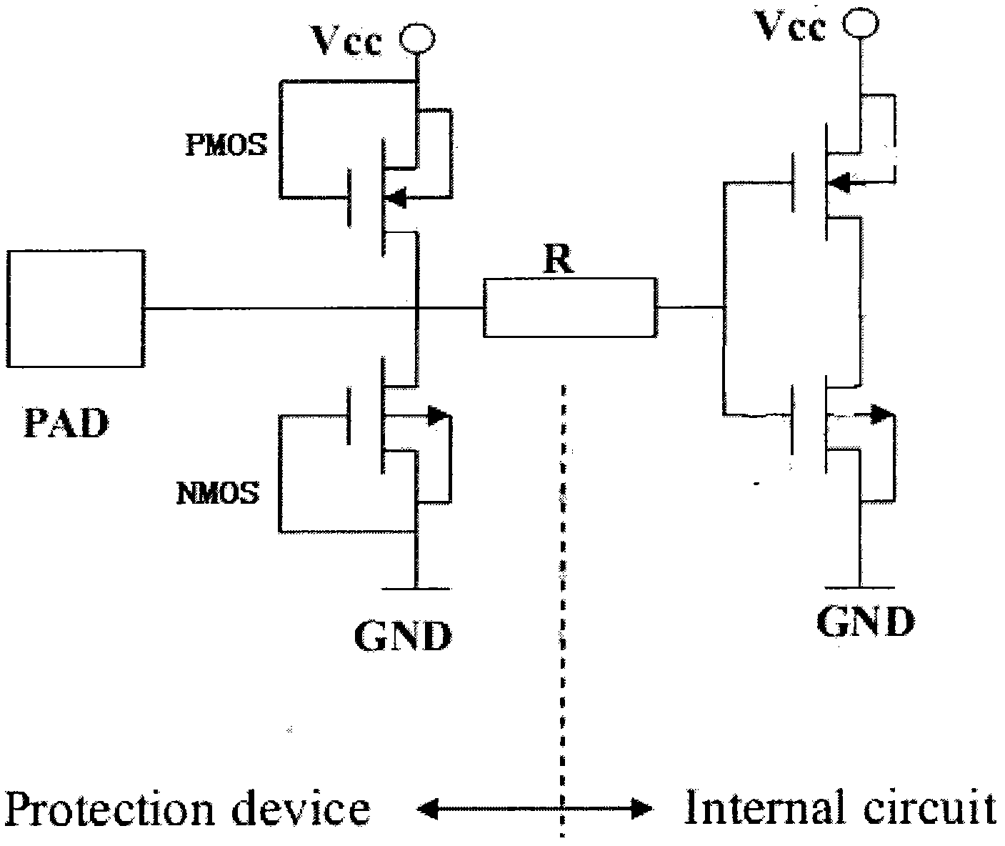
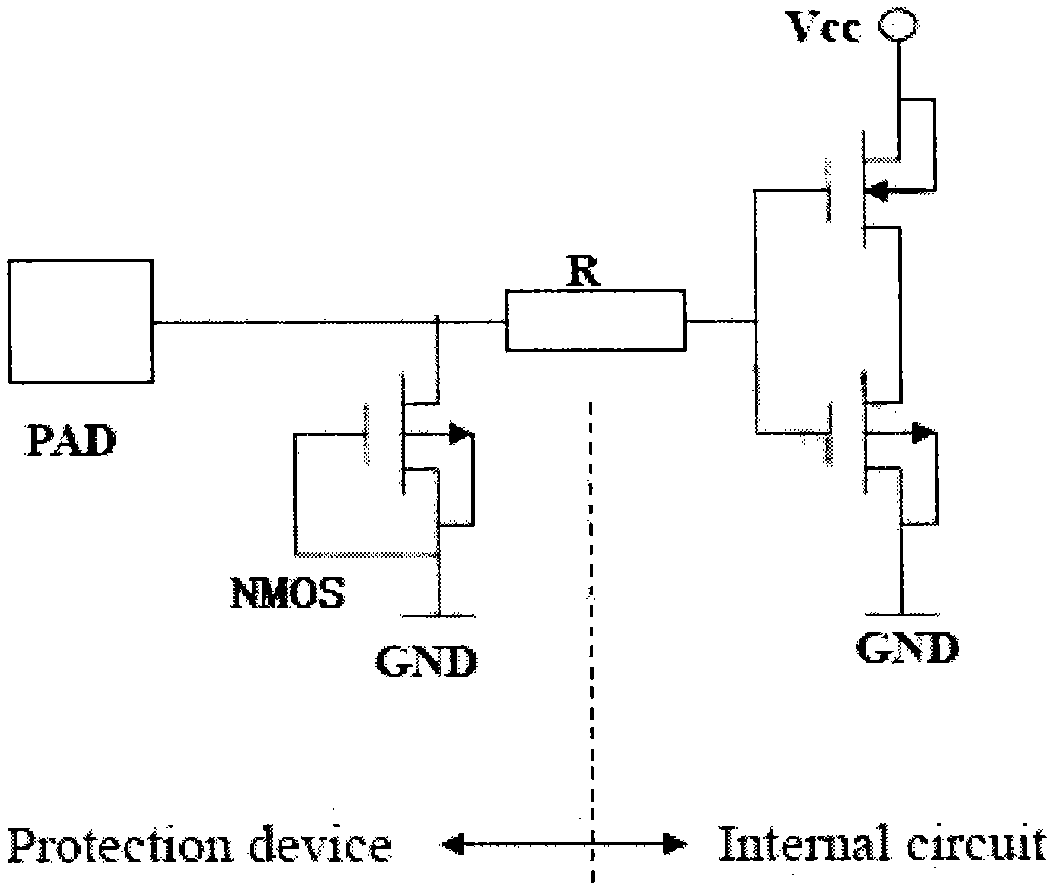
[0021] figure 1 For the circuit diagram of the prior art, electrostatic protection is performed by connecting a PMOS transistor and an NMOS transistor. figure 2 It is a circuit diagram of an embodiment of the present invention. The gate terminal, the P-type substrate and the source terminal of the NMOS transistor are connected and grounded, and the drain terminal is connected to the PAD; one end of the resistor is connected to the PAD, and the other end is the output terminal of the electrostatic protection structure, which is connected to the internal circuit. . Compared with the prior art, the present invention obviously omits one PMOS transistor and greatly reduces the chip area.

[0022] In order to further reduce the chip area without affecting the effect of electrostatic protection, the present invention further improves the layout design. Figure 4 For the layout of the NMOS tube, the distance from the through hole at the source end to the gate end is 1 μm, and the d...

Embodiment 2

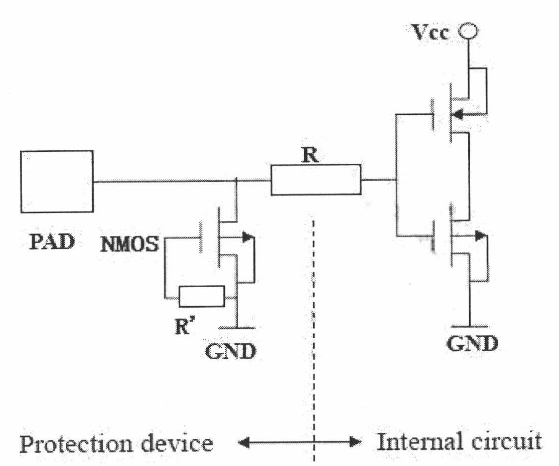
[0024] image 3 It is a circuit diagram of another embodiment of the present invention. The structure and principle of this embodiment are basically the same as those of the first embodiment. The difference is that another resistor R' is added between the gate terminal of the NMOS transistor and the ground. The reason is that not every NMOS transistor will be turned on at the same time when ESD occurs, so the effective withstand voltage of the ESD protection circuit is determined by several NMOS transistors that start to conduct. Adding another resistor R' between the gate terminal of the NMOS transistor and the ground can effectively avoid this situation.


PUM


Abstract

The invention provides an electrostatic protection structure. The electrostatic protection structure consists of an N-channel metal-oxide semiconductor (NMOS) transistor, a resistor and a pressure welding pad, wherein the gate end, a P-type substrate and a source end of the NMOS transistor are connected and are grounded; the drain end is connected with the pressure welding pad; one end of the resistor is connected with the pressure welding pad; the other end is the output end of the electrostatic protection structure and is connected with an internal circuit of a chip; the NMOS transistor also comprises an N-type diffusion area, polysilicon, a source-end substrate leading-out wire and an isolation ring; the overlapping part of the polysilicon and the N-type diffusion area forms the gate end; the N-type diffusion area comprises N-traps on the P-type substrate; the source end and the drain end are both formed by the N-traps and are in interdigital crisscross distribution; through holes are reserved in the N-traps in which the source end and the drain end are positioned; the through hole of the source end is connected with the source-end substrate leading-out wire; the isolation ring is connected with the source end; the source-end substrate leading-out wire is also connected with the P-type substrate; the resistor is formed by the polysilicon; and the polysilicon is directly connected with the pressure welding pad. The electrostatic protection structure can greatly improve electrostatic discharge (ESD) capacity, shorten chip area and reduce chip cost, and does not influence chip performance without changing process conditions.

Description

technical field [0001] The present invention relates to an integrated circuit, in particular to an electrostatic protection structure of a chip, and is particularly suitable for saving chip area. Background technique [0002] With the rapid development of integrated circuits, the issue of how to control costs has also been put on the table. For designers, the control of chip area is the most prioritized and effective method. And people's requirements for chips are getting higher and higher. In the application process of the chip, people hope that the function of the chip is not only correct, but also improves the performance requirements of the chip. [0003] Electrostatic discharge (ESD, Electrostatic Discharge) is a major factor that causes electronic components or electronic systems to be damaged by excessive electrical stress (Electrical Over Stress, EOS). Among the various means of electrostatic protection, the most important and most effective way is to integrate the...

Claims


Application Information

Patent Timeline
Patent Type & Authority Applications(China)
IPC IPC(8): H01L27/02H01L29/78H01L29/06
Inventor 杭晓伟彭秋平贾力张祯
Owner SUZHOU HUAXIN MICROELECTRONICS
Learn More