Formation method of otp device

A device and patterning technology, used in semiconductor/solid-state device manufacturing, electrical components, circuits, etc., to solve the problems of particle pollution, easy peeling off of photoresist layers, etc.

Active Publication Date: 2015-12-02
SHANGHAI HUAHONG GRACE SEMICON MFG CORP
View PDF6 Cites 0 Cited by
  • Summary
  • Abstract
  • Description
  • Claims
  • Application Information

AI Technical Summary

Problems solved by technology

[0009] The problem solved by the invention is that the photoresist layer is easy to peel off during the formation of the OTP device, resulting in the problem of particle pollution

Method used


Image

  • Formation method of otp device
  • Formation method of otp device
  • Formation method of otp device

Examples


Embodiment Construction

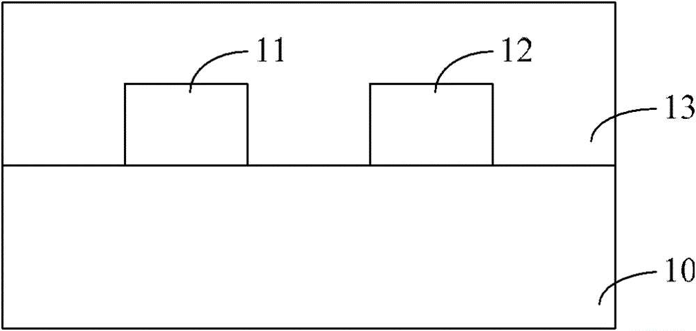
[0034] In the prior art, due to poor adhesion between the photoresist layer and the dielectric layer, it is easy to fall off during the wet etching process, resulting in particle pollution.

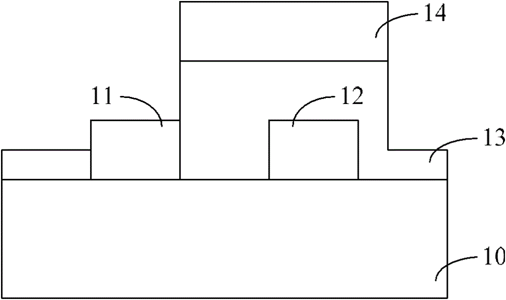
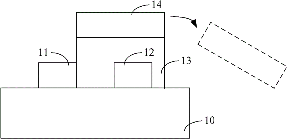
[0035] This technical scheme first introduces nitrogen element on the surface of the dielectric layer covering the floating gate and the selection gate, and then forms a patterned photoresist on it, thereby effectively improving the performance of the dielectric layer and patterned photolithography. The adhesion between the glues avoids the problem of particle contamination caused by the peeling off of the patterned photoresist during the wet etching process. In addition, it can also avoid the damage of the dielectric layer above the floating gate and prevent the data of the OTP device from being damaged. Retention is affected.

[0036] In order to make the above objects, features and advantages of the present invention more comprehensible, specific implementations of the present inventio...


PUM


Abstract

The invention relates to a formation method of an OTP (One Time Programmable) device, comprising the following steps of: providing a semiconductor substrate, wherein a selective gate and a floating gate are formed on the semiconductor substrate in parallel; forming a dielectric layer, and covering the selective gate, the floating gate and the surface of the semiconductor substrate; introducing a nitrogen element to the surface of the dielectric layer; forming a patterned photoresist on the surface of the dielectric layer, wherein the patterned photoresist covers the dielectric layer over the floating gate; and etching the dielectric layer with the patterned photoresist as a mask, and exposing the selective gate and the surface of the semiconductor substrate. The formation method of the OTP device can improve the adhesion of the dielectric layer and the patterned photoresist, avoid the particle pollution problem caused by the peeling and the falling of the patterned photoresist and also avoid influence on data storage capacity of the OTP device.

Description

technical field [0001] The invention relates to the technical field of semiconductors, in particular to a method for forming an OTP device. Background technique [0002] A one-time programmable (OTP, OneTime Programmable) device is a commonly used memory, which belongs to a read-only memory. It is named because it can only be programmed once. When the OTP device leaves the factory, the general storage content is 0 or 1. Users can program it according to their own needs and write user data. Due to the advantages of simple structure, easy to use, and low cost, OTP devices can replace traditional electrically erasable memory (EPROM) in chips such as microcontrollers (MCU, MicroControlUnit), and are widely used. [0003] Figure 1 to Figure 3 A method for forming an OTP device in the prior art is shown. [0004] refer to figure 1 , providing a semiconductor substrate 10, on which a selection gate (SG, SelectiveGate) 11 and a floating gate (FG, FloatingGate) 12 are formed sid...

Claims


Application Information

Patent Timeline
Patent Type & Authority Patents(China)
IPC IPC(8): H01L21/8247H01L21/3115H01L21/311
Inventor 孙凌
Owner SHANGHAI HUAHONG GRACE SEMICON MFG CORP
Why Eureka
Try Eureka