
Broadband read-write memory apparatus

A memory and readout device technology, applied in the direction of read-only memory, static memory, digital memory information, etc., can solve the problems of increasing the number of SRAM unit word lines and bit lines, SRAM unit layout area, control complexity design and manufacturing cost, etc.

Active Publication Date: 2011-06-29
SHANGHAI XINHAO MICROELECTRONICS
View PDF3 Cites 12 Cited by
  • Summary
  • Abstract
  • Description
  • Claims
  • Application Information

AI Technical Summary

Problems solved by technology

For multi-port SRAM memory, multiple read and write operations can be completed in one clock cycle, but at the expense of increasing the number of SRAM cell word lines and bit lines, SRAM cell layout area, control complexity, design and manufacturing costs

Method used

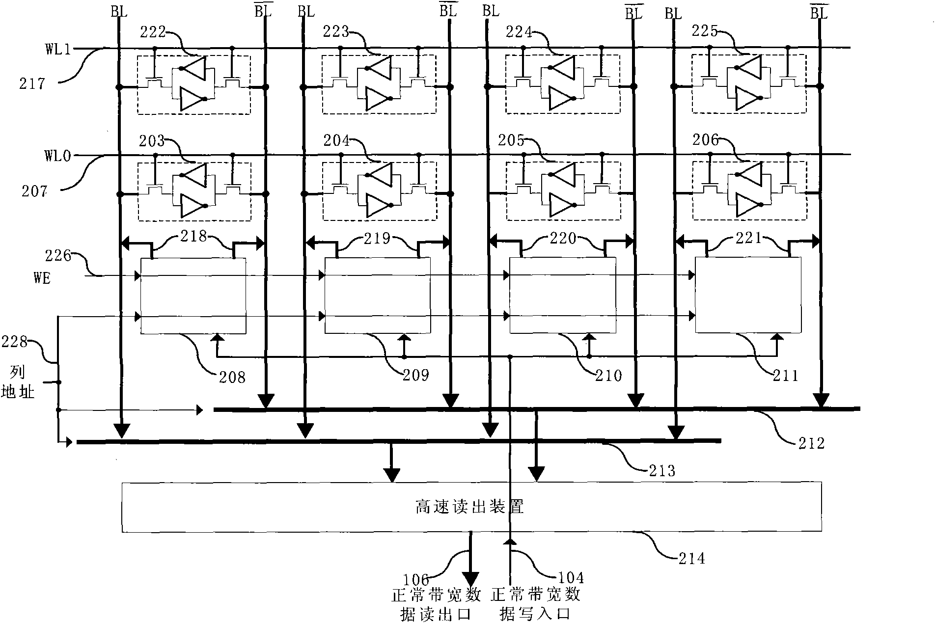
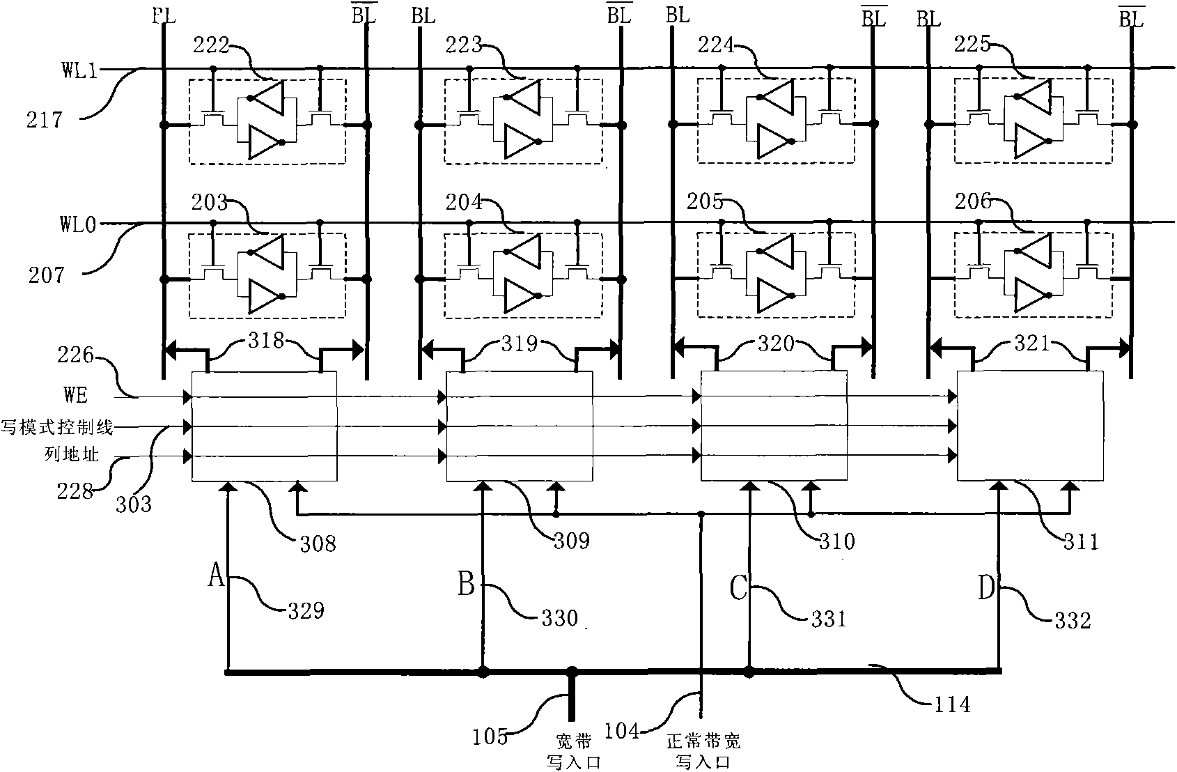

Image

  • Broadband read-write memory apparatus
  • Broadband read-write memory apparatus
  • Broadband read-write memory apparatus

Examples


Embodiment Construction

[0026] In order to make the object, technical solution and advantages of the present invention more clear, the present invention will be further described in detail below in conjunction with the accompanying drawings and embodiments. It should be understood that the specific embodiments described here are only used to explain the present invention, and are not intended to limit the present invention. For those skilled in the art, various possible replacements, adjustments and improvements can be made according to the technical scheme and concept of the present invention, and all these replacements, adjustments and improvements should belong to the protection scope of the appended claims of the present invention.

[0027] The technical idea of ​​the invention is to increase the writing and reading bandwidth of the memory by increasing the writing and reading ports or changing the reading and writing sequence.

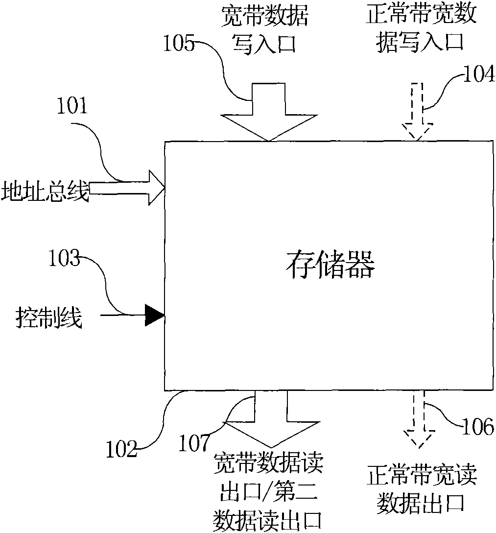
[0028] see figure 1 , which is a system input and output interface...


PUM


Abstract

The invention belongs to the field of designing of integrated circuits and provides a read-write bandwidth improvement memory apparatus. Particularly, a broadband data read-write port, besides a normal read-write port, is arranged on a memory in four modes, namely a wide bandwidth read mode, a normal bandwidth read mode, a wide bandwidth write mode and a normal bandwidth write mode. Different columns of memory units, which share word lines, of a memory array can pass through a broadband data write-in port and perform write-in operation simultaneously; and after values in the memory units corresponding to an input address is read out during read-out, values inside all other columns of memory units which share the word lines can be read out through a broadband data read-out port. Write-after-read operation can be performed on different memory rows of the memory array in the same clock period. A plurality of memory arrays can share a group of read-out apparatuses, and read-write operation in different arrays can be performed simultaneously.

Description

technical field [0001] The invention relates to the field of integrated circuit design, and relates to a method and a device for improving memory read and write bandwidth through structure optimization. Background technique [0002] With the advancement of technology and the increase of actual demand, in the field of storage circuit design, the scale of memory arrays is getting larger and larger. Usually, the physical layout of the memory array is rectangular, and the layout area of ​​the readout device occupies a considerable part of the chip area of ​​the entire memory. Logically, memory cells in several different columns usually share a word line. Traditional memory read and write methods write or read a set of data for each clock cycle. Taking a 512X32-bit single-port static random access memory (SRAM) array as an example, the SRAM array at the physical level is usually designed as 128 rows, and each row has 4X32 SRAM cells. Group readout device. [0003] When writing...

Claims


Application Information

Patent Timeline
IPC IPC(8): G11C7/12G11C11/4063
CPCG11C16/10G11C16/26G11C16/08G11C7/10G11C7/1075G11C8/16G11C11/419
Inventor 林正浩张冰淳
Owner SHANGHAI XINHAO MICROELECTRONICS
Learn More