Surface processing method of PCB (printed circuit board)
A printed circuit board and surface treatment technology, which is applied in the secondary treatment of printed circuit, the reinforcement of conductive patterns, etc., can solve the problems of increasing the cost of surface treatment of printed circuit boards, and achieve the effect of reducing the use of gold and reducing costs
Active Publication Date: 2011-06-15
SHENNAN CIRCUITS
View PDF2 Cites 10 Cited by
- Summary
- Abstract
- Description
- Claims
- Application Information
AI Technical Summary
Problems solved by technology
In the electroplating hard gold process and electroplating soft gold process, in order to ensure the wire bonding performance of soft gold and the wear resistance of hard gold, the thickness of the gold layer is required to be above 0.5 μm. Increased cost of surface treatment of printed circuit boards
Method used
View moreImage
Smart ImageViewing Examples

Examples
Embodiment Construction
Login to View More PUM
| Property | Measurement | Unit |
|---|---|---|
| thickness | aaaaa | aaaaa |
Abstract
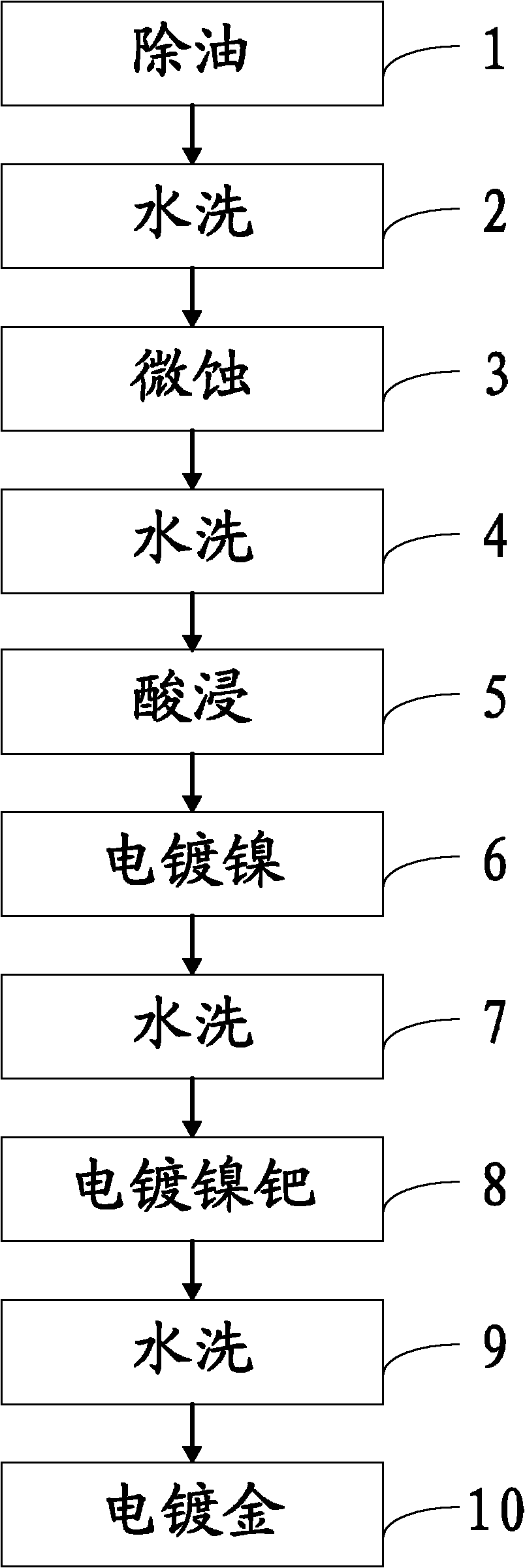
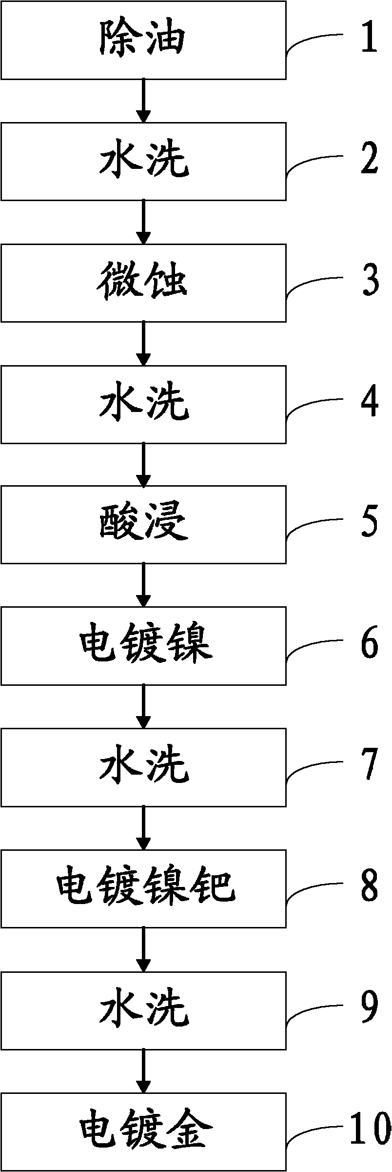
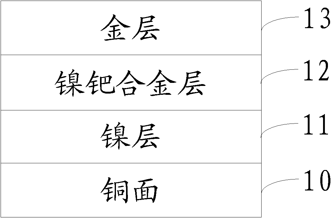
The invention discloses a surface processing method of a PCB (printed circuit board), mainly comprising the following steps: electroplating nickel, and evenly coating a layer of metal nickel on the PCB; electroplating a nickel palladium alloy, and coating a layer of nickel palladium alloys on the nickel surface of the PCB, wherein as for the liquid medicine, the temperature of the liquid medicineis 60-64 DEG C, the concentration of palladium ions is 6-9 g / L, the concentration of nickel ions is 5-8 g / L, and the PH value is 4.6-5.8; and electroplating aurum, coating an aurum layer with the thickness of 0.1 mu m on the nickel palladium alloy surface of the PCB. A step of electroplating the nickel palladium alloys is added between the step of electroplating nickel and the step of electroplating aurum, so that the circuit board is sequentially coated with a nickel layer, a nickel palladium alloy layer and an aurum layer. As the nickel palladium alloy has excellent performance, and the nickel palladium alloy is used as the intermediate layer between the nickel and the aurum, the usage amount of aurum is reduced. The method provided the invention can reduce the cost under the condition of not affecting aurum wiring performance and wearing performance.
Description
Surface treatment method of a printed circuit board technical field The invention relates to the field of printed circuit board manufacturing, and more specifically, relates to a surface treatment method for a printed circuit board. Background technique The Chinese name of PCB (Printed Circuit Board) is a printed circuit board. On an insulating substrate, according to a predetermined design, a printed circuit, a printed component, or a combination of the two is formed by using metal copper to form a specific conductive pattern. One of the important components of the electronics industry. Although the metal copper of the printed circuit board is a good component soldering surface and electrical signal transmitter, the metal copper is easily oxidized when exposed to the air, and copper oxide will hinder the wetting and conductivity of the solder, so it is usually used on copper Coated with a stable substance, such as nickel and gold on copper. Gold is the most widely used ...
Claims
Login to View More Application Information
Patent Timeline
 Patent Type & Authority Applications(China)
IPC IPC(8): H05K3/24
Inventor 罗威
Owner SHENNAN CIRCUITS
Features
- R&D
- Intellectual Property
- Life Sciences
- Materials
- Tech Scout
- Unparalleled Data Quality
- Higher Quality Content
- 60% Fewer Hallucinations
Learn More Browse by: Latest US Patents, China's latest patents, Technical Efficacy Thesaurus, Application Domain, Technology Topic, Popular Technical Reports.
© 2025 PatSnap. All rights reserved.Legal|Privacy policy|Modern Slavery Act Transparency Statement|Sitemap|About US| Contact US: help@patsnap.com