Contact image sensing module
A sensor module and contact technology, applied in image communication, electrical components, etc., can solve the problems of low space utilization rate and uncompact image sensor structure, etc., and achieve compact structure, reduced space occupation, and uniform illumination Effect
- Summary
- Abstract
- Description
- Claims
- Application Information
AI Technical Summary
Problems solved by technology
Method used
Image
Examples
Embodiment Construction
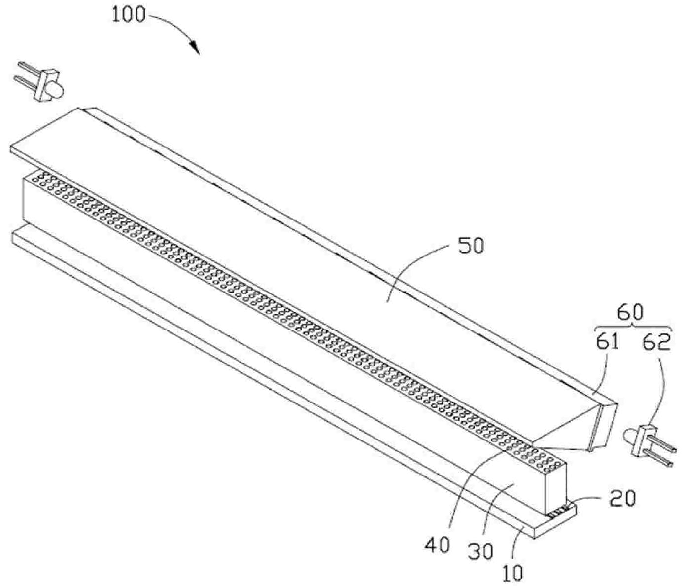
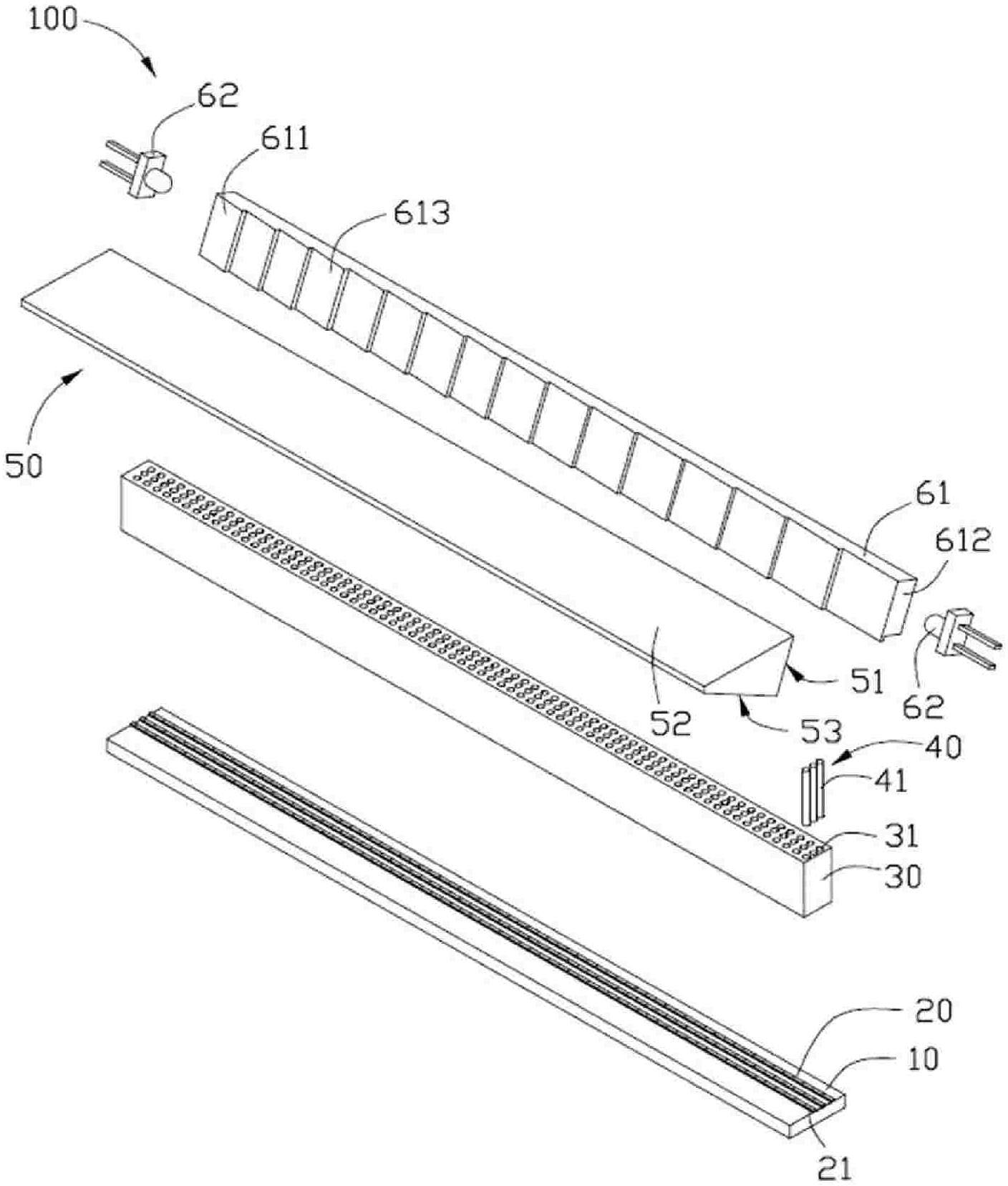
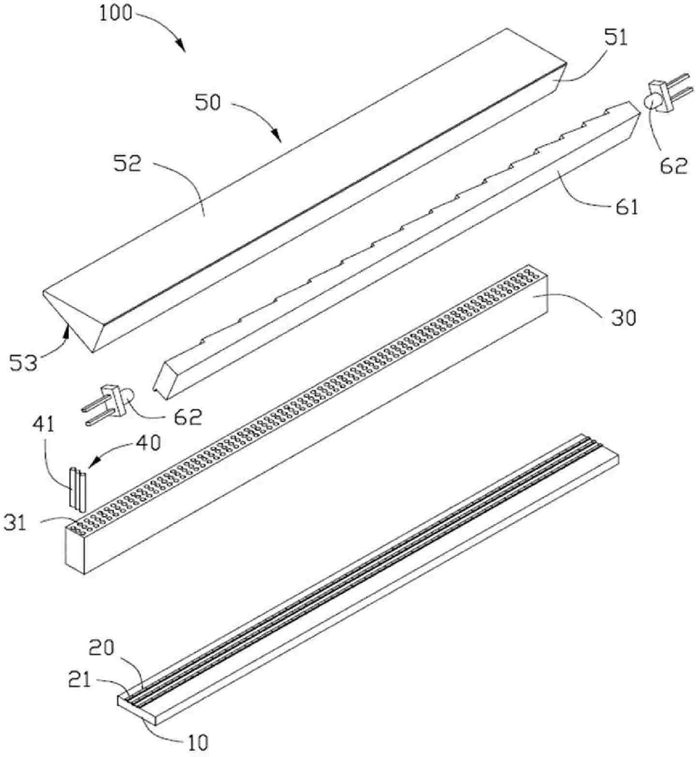
[0014] Such as Figure 1 to Figure 4 Shown is a preferred embodiment of the contact image sensor module 100 of the present invention. The contact image sensor module 100 includes a circuit board 10 , a contact image sensor element 20 , a bearing seat 30 , a lens group 40 , a glass plate 50 and an LED light source 60 . These components of the contact image sensor module 100 can be disposed together in a scanner or a fax machine housing (not shown).
[0015] The circuit board 10 is elongated and placed horizontally, and the contact image sensing element 20 is disposed on the circuit board 10 . The contact image sensing device 20 includes a plurality of contact image sensors 21 arranged in three rows along the lengthwise direction of the circuit board 10 .
[0016] The carrying seat 30 is located above the circuit board 10 , and the carrying seat 30 is elongated and has a rectangular cross section. The bearing base 30 is provided with a plurality of through holes 31 extending ...
PUM
 Abstract
Description
Claims
Application Information
 - R&D
- Intellectual Property
- Life Sciences
- Materials
- Tech Scout
- Unparalleled Data Quality
- Higher Quality Content
- 60% Fewer Hallucinations
Browse by: Latest US Patents, China's latest patents, Technical Efficacy Thesaurus, Application Domain, Technology Topic, Popular Technical Reports.
© 2025 PatSnap. All rights reserved.Legal|Privacy policy|Modern Slavery Act Transparency Statement|Sitemap|About US| Contact US: help@patsnap.com


