PECL (Positive Emitter Coupling Logic) level interface circuit
An interface circuit and level technology, applied in the direction of logic circuit connection/interface layout, etc., can solve the problems of unsatisfactory common mode level and large output impedance, and achieve the effects of high precision, high reliability and simple circuit structure.
- Summary
- Abstract
- Description
- Claims
- Application Information
AI Technical Summary
Problems solved by technology
Method used
Image
Examples
Embodiment 1
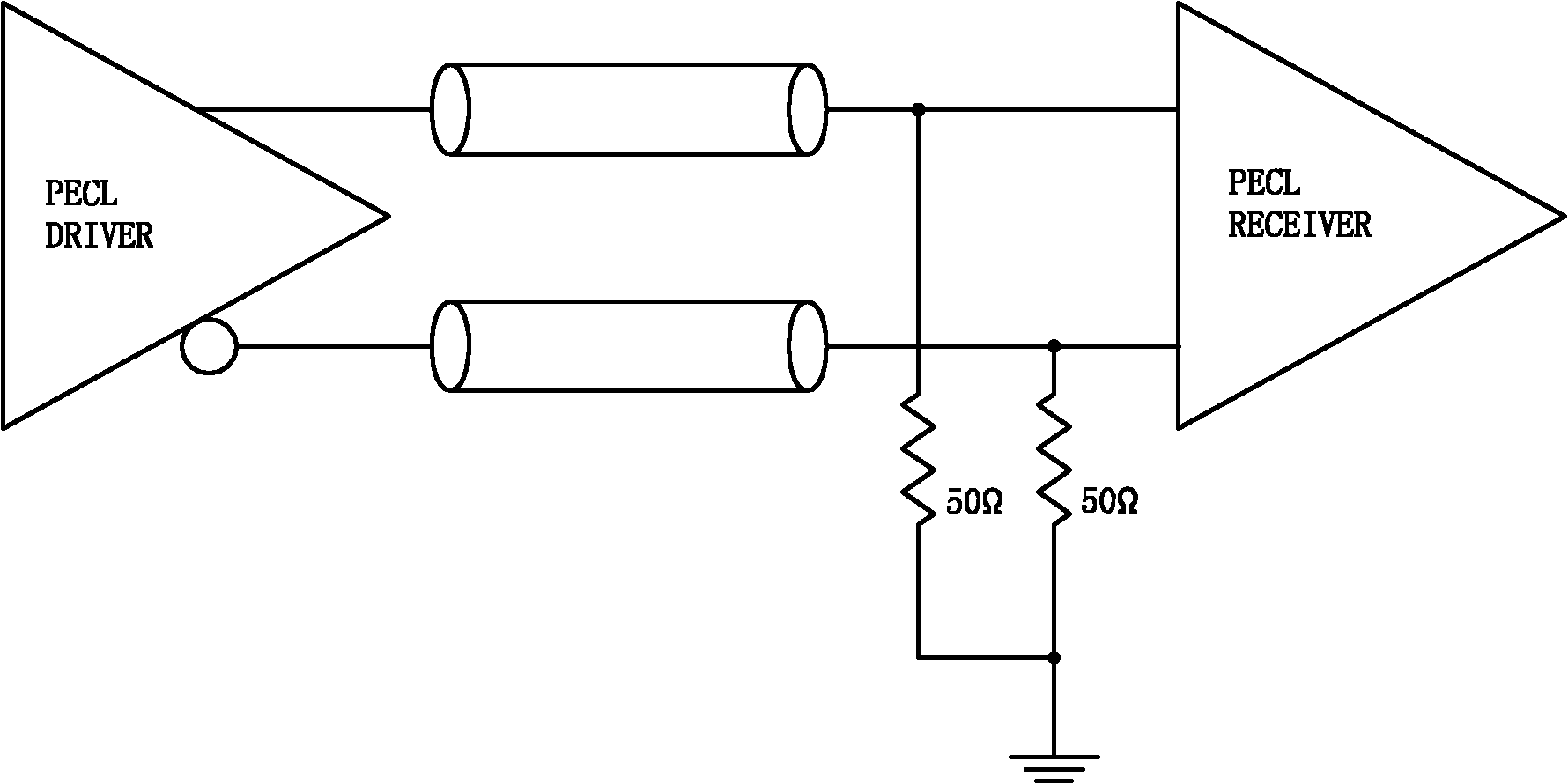
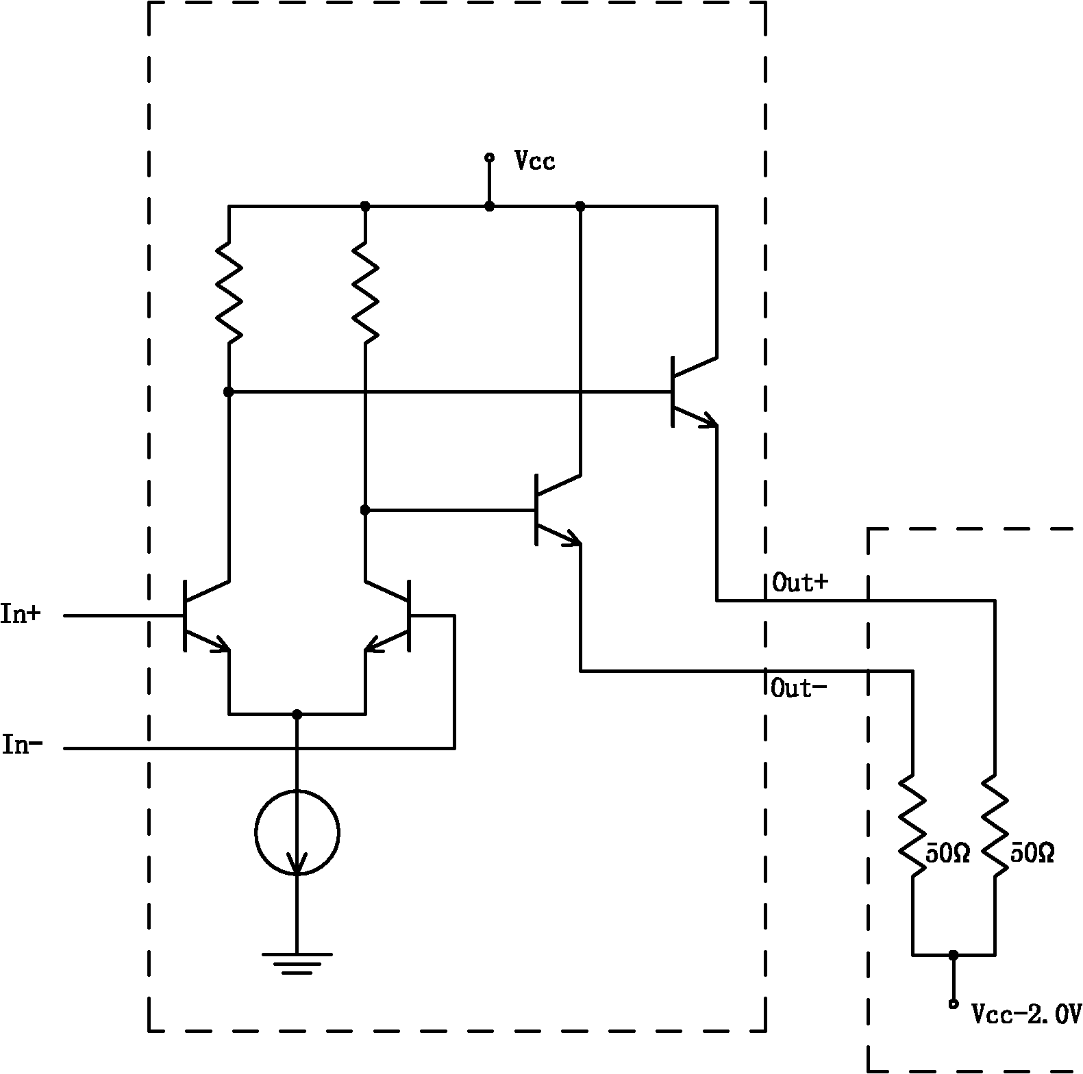
[0039] figure 1 It is the equivalent schematic diagram of Dai Wenning defined by the PECL standard. For a differential load with an AC load impedance of 50Ω, the common-mode level of the output node is maintained at VCC-1.3V, and the differential output amplitude is about 1.4Vpp. Generally, it is implemented as figure 2 As shown, it is a PECL output circuit with a traditional open-emitter structure, and this structure is also the origin of the name of the PECL interface. The output impedance of the transistor with the open emitter structure is relatively low, and it works in an amplified state. Therefore, the circuit with this structure can meet the common-mode voltage requirement of Vcc-1.3V while driving various specific load forms. However, if such a structure is realized by CMOS technology, the gate, drain and source of the MOS are simply replaced with the base, collector and emitter of the transistor, even if the bias of the appropriate MOS transistor is used, the It c...
Embodiment 2
[0042] Figure 4It is the circuit diagram of the voltage generator in the common mode negative feedback module of the second embodiment of the present invention; the function of the voltage generator is to generate a Vcc-1.3V reference voltage following Vcc; the voltage generator adopts the reference voltage 1.2V under the CMOS process V is a reference reference, and then a constant current branch is formed by the comparator A1, the adjustment tube M0 and the resistor R0, and the reference reference flows through R0 to obtain a constant current, and the mirror current source including M1, M2, and M3 will This constant current is mirrored to R1, and finally Vref following Vcc is obtained from the low potential end of R1. The relationship between R0 and R1 is determined as: R1 / R0=1.3 / 1.2, then Vref=Vcc-1.3V can be obtained, and the Vref precision of this structure is higher.
[0043] Such as Figure 5 , the circuit diagram of the negative feedback driver in the common mode neg...
PUM
 Abstract
Description
Claims
Application Information
 - R&D Engineer
- R&D Manager
- IP Professional
- Industry Leading Data Capabilities
- Powerful AI technology
- Patent DNA Extraction
Browse by: Latest US Patents, China's latest patents, Technical Efficacy Thesaurus, Application Domain, Technology Topic, Popular Technical Reports.
© 2024 PatSnap. All rights reserved.Legal|Privacy policy|Modern Slavery Act Transparency Statement|Sitemap|About US| Contact US: help@patsnap.com


