Liquid crystal display panel and manufacturing method thereof
A technology of a liquid crystal display panel and a manufacturing method, which is applied to static indicators, nonlinear optics, instruments, etc., can solve the problems of scratches on touch circuits, not easy to scratch on touch circuits, etc., and achieves the effect of protecting foreign objects from scratches
- Summary
- Abstract
- Description
- Claims
- Application Information
AI Technical Summary
Problems solved by technology
Method used
Image
Examples
Embodiment Construction
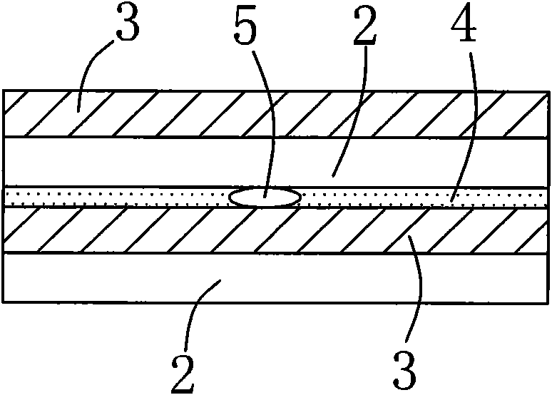
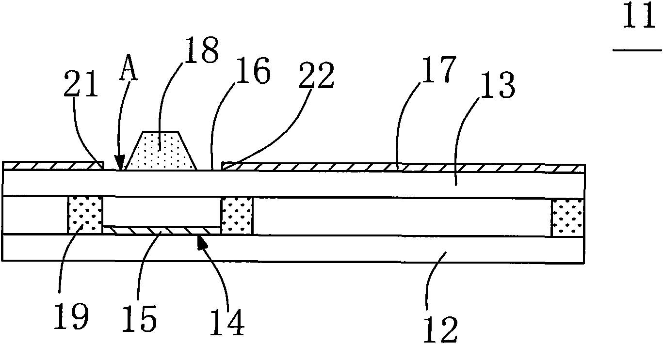
[0024] See figure 2 and image 3 , figure 2 Shown is a schematic diagram of a display substrate according to the present invention, image 3 Shown is a schematic diagram of display substrates stacked according to the present invention. The liquid crystal display panel is formed by cutting a display substrate 11 , and the display substrate 11 includes a first substrate 12 and a second substrate 13 opposite to the first substrate 12 . The first substrate 12 is a thin film transistor array substrate, and the second substrate 13 is a color filter substrate. Wherein, the liquid crystal display panel is a touch panel. Moreover, a sealant 19 is provided between the first substrate 12 and the second substrate 13 of the display substrate 11 to seal the liquid crystal layer between the first substrate 12 and the second substrate 13 .
[0025] The first surface 14 of the first substrate 12 has external pin lines 15, the second surface 16 of the second substrate 13 facing away from...
PUM
 Abstract
Description
Claims
Application Information
 - R&D Engineer
- R&D Manager
- IP Professional
- Industry Leading Data Capabilities
- Powerful AI technology
- Patent DNA Extraction
Browse by: Latest US Patents, China's latest patents, Technical Efficacy Thesaurus, Application Domain, Technology Topic, Popular Technical Reports.
© 2024 PatSnap. All rights reserved.Legal|Privacy policy|Modern Slavery Act Transparency Statement|Sitemap|About US| Contact US: help@patsnap.com


