Method for making and packaging printed circuit board (PCB) and crystal oscillator

A technology for printed circuit boards and crystal oscillators, which can be used in printed circuit manufacturing, printed circuits, and electrical components to assemble printed circuits. Good shielding performance, convenient and accurate positioning and installation and fixing, and the effect of improving product production efficiency

Active Publication Date: 2011-05-18
GUANGDONG DAPU TELECOM TECH CO LTD
View PDF5 Cites 11 Cited by
  • Summary
  • Abstract
  • Description
  • Claims
  • Application Information

AI Technical Summary

Problems solved by technology

However, in the process of PCB board processing, such as reflow soldering of surface mount components, the positioning and fixing method of the metal cover has become a difficult problem in the industry. At present, the fixing method of the metal cover on the market adopts the direct welding method, which is expensive. , and the defective rate is high, which is not conducive to the realization of high-efficiency and high-quality PCB board manufacturing process

Method used


Image

  • Method for making and packaging printed circuit board (PCB) and crystal oscillator
  • Method for making and packaging printed circuit board (PCB) and crystal oscillator
  • Method for making and packaging printed circuit board (PCB) and crystal oscillator

Examples


Embodiment Construction

[0023] Embodiments of the present invention will now be described with reference to the drawings, in which like reference numerals represent like elements. The invention provides a printed circuit board manufacturing method and a packaging method thereof capable of improving product production efficiency and product quality, and a crystal oscillator with the printed circuit board, so as to realize flexible manufacturing and assembly of the crystal oscillator and modification.

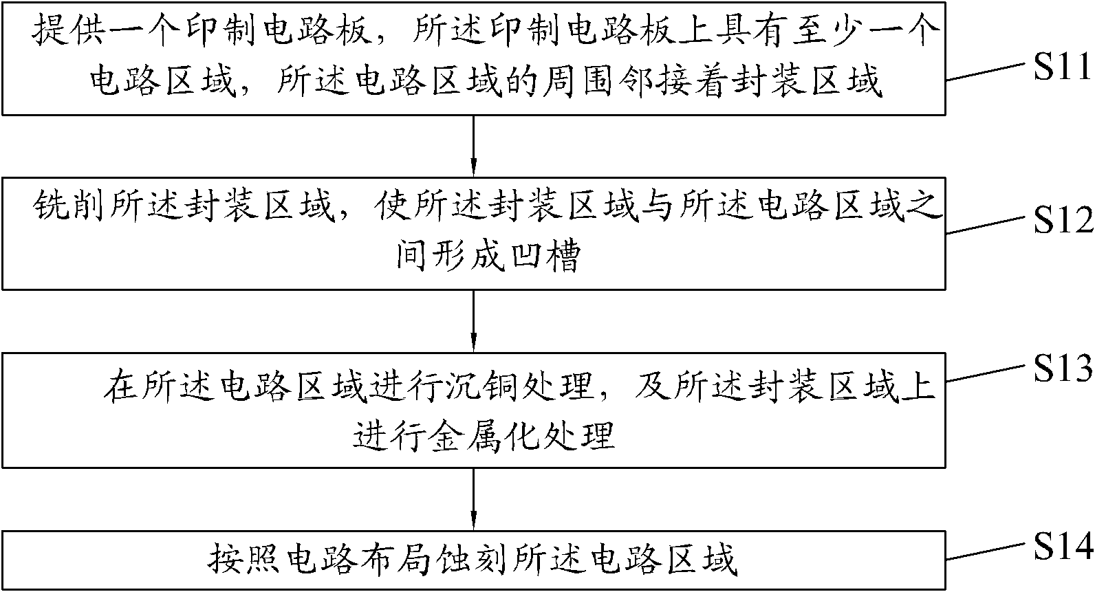
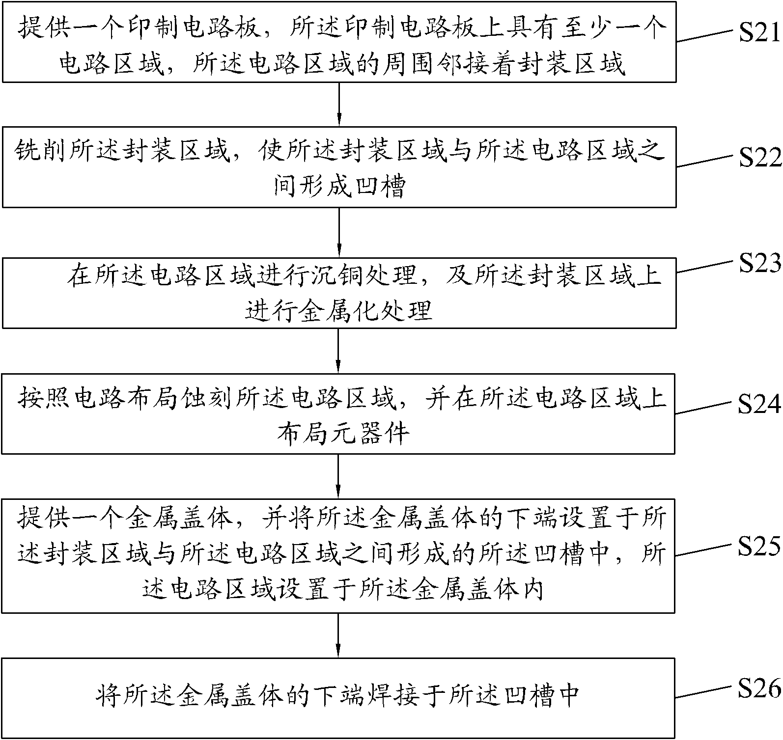
[0024] Such as figure 1 Shown is a flow chart of the method for manufacturing a printed circuit board of the present invention, the steps of the method are as follows: step S11, providing a printed circuit board, the printed circuit board has at least one circuit area, the circuit area The surrounding area is adjacent to the package area; step S12, milling the package area, so that a groove is formed between the package area and the circuit area; step S13, performing copper sinking treatment on the cir...


PUM


Abstract

The invention discloses a method for making and packaging a printed circuit board (PCB). The method comprises the following steps of: providing the PCB, wherein, the PCB is provided with at least one circuit area, and a packaging area is closely arranged around the circuit area; milling the packaging area so as to form a groove between the packaging area and the circuit area; carrying out electroless copper plating in the circuit area and metallization treatment in the packaging area; etching the circuit area according to circuit layout, and arranging components on the circuit area; providing a metal cover body, arranging the lower end of the metal cover body in the groove formed between the packaging area and the circuit area, wherein the circuit area is in the metal cover body; and welding the lower end of the metal cover body with the groove. The invention further discloses a crystal oscillator with the PCB.

Description

technical field [0001] The invention relates to the field of printed circuit boards, in particular to a method for manufacturing a printed circuit board, a packaging method, and a crystal oscillator with the printed circuit board. Background technique [0002] In electronic products and related industries (such as the crystal oscillator industry), various electronic components need to be electrically connected to transmit power signals, data signals, etc. Packaging is critical. Based on some devices with relatively little usage and high frequency and high stability, it is difficult to realize chip-scale packaging. Usually, the manufacturers of related products will arrange the circuits with specific functions on a printed circuit board (PCB board), and after debugging and testing, they will be packaged into a single device for sale. Now the production process is mainly surface mount, so after the product is formed, the surface mount device is the main one. Surface mount d...

Claims


Application Information

Patent Timeline
Patent Type & Authority Applications(China)
IPC IPC(8): H05K3/30H05K3/00H01L21/50H03H9/02
Inventor 刘朝胜
Owner GUANGDONG DAPU TELECOM TECH CO LTD
Why Eureka
Try Eureka