Method for separating sapphire substrate by unit on basis of stress action

A sapphire substrate, stress-action technology, applied in electrical components, semiconductor/solid-state device manufacturing, circuits, etc., can solve the problem of low yield of laser lift-off, and achieve the effect of ensuring unit independence and improving yield

Active Publication Date: 2013-05-01
FUJIAN JING AN OPTOELECTRONICS CO LTD
View PDF0 Cites 0 Cited by
  • Summary
  • Abstract
  • Description
  • Claims
  • Application Information

AI Technical Summary

Problems solved by technology

[0005] In order to solve the above-mentioned problem of low laser lift-off yield, the present invention innovatively proposes a stress-based method for separating sapphire substrates unit by unit, including the following steps:

Method used


Image

  • Method for separating sapphire substrate by unit on basis of stress action
  • Method for separating sapphire substrate by unit on basis of stress action
  • Method for separating sapphire substrate by unit on basis of stress action

Examples


Embodiment Construction

[0023] The present invention will be further described below in conjunction with the accompanying drawings and embodiments.

[0024] A method for separating a sapphire substrate unit by unit based on stress, the preparation steps are as follows:

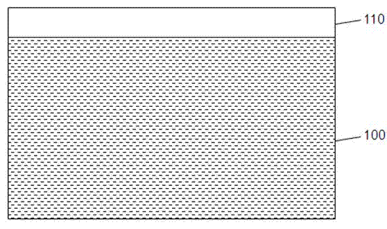
[0025] Such as figure 2 As shown, an N-type GaN-based semiconductor layer, an active layer and a P-type GaN-based semiconductor layer are epitaxially grown sequentially on a sapphire substrate 100 by metal organic chemical vapor deposition (MOCVD) to form a GaN-based epitaxial thin film 110 .

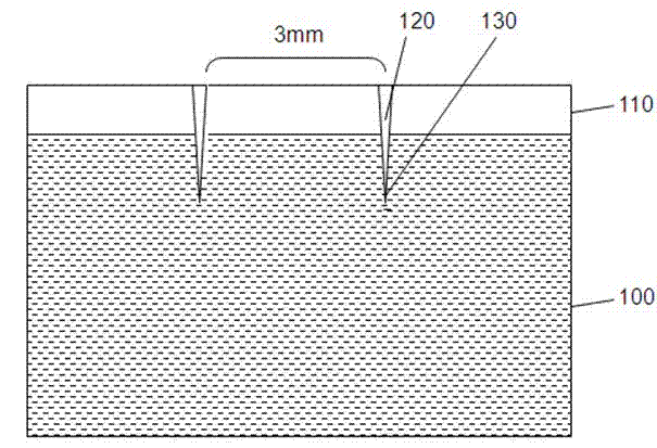
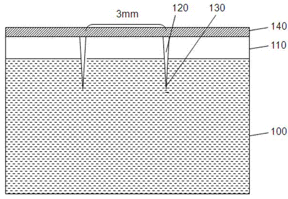
[0026] Such as image 3 As shown, a laser scribing machine (wavelength 355nm) is used to slit the GaN-based epitaxial film 110 and extend it to the sapphire substrate 100. The scribing is carried out in an orthogonal (X-Y axis) manner with a period of 3mm×3mm, and the set The size of the laser lift-off spot is similar, and the depth of laser scribing is 30 microns, that is, to realize the unitization of GaN-based epitaxial thin films, the g...


PUM


Abstract

The invention discloses a method for separating a sapphire substrate by unit on basis of stress action, comprising the following steps: adopting a first type of laser to realize the unit isolation of GaN base epitaxy; ensuring the unit independency of the GaN base epitaxy; meanwhile, utilizing a second type of laser to scan the upper tangential stress between the unit sapphire substrate and adjacent non-scanning unit sapphire substrate; and under the combined action of GaN interface nitrogen pressure and the upper tangential stress, separating and removing the sapphire substrate by unit. Thus, laser stripping finished product rate can be obviously improved.

Description

technical field [0001] The invention relates to a method for removing a sapphire substrate by using a laser lift-off technique, and more specifically relates to a method for separating a gallium nitride-based epitaxial layer from a sapphire substrate. Background technique [0002] At present, most gallium nitride (GaN)-based epitaxial materials are mainly grown on sapphire substrates, and high crystal quality can be obtained through the introduction of buffer layers, so that GaN-based materials can be widely used in various optoelectronic devices and electronic devices. However, the poor material properties of sapphire itself hinder the manufacturing and performance improvement of GaN-based devices. On the one hand, the insulating properties of the sapphire substrate make GaN-based devices generally adopt a lateral structure, that is, different electrodes are fabricated on the same side of the device, which requires the introduction of etching and other processes, which inc...

Claims


Application Information

Patent Timeline
Patent Type & Authority Patents(China)
IPC IPC(8): H01L21/86H01L21/30
Inventor 林雪娇林科闯蔡文必
Owner FUJIAN JING AN OPTOELECTRONICS CO LTD
Why Eureka
Try Eureka