Three-dimensional light-emitting led chip filament and led bulb

A technology of LED chips and filaments, which is applied to semiconductor devices, electric solid-state devices, electrical components, etc., can solve the problems of affecting the quality of the lamp body, difficult to fix the leads, difficult to weld and connect, etc. The effect of simplifying the stand

Inactive Publication Date: 2016-05-25
DONGGUAN QIJIA ELECTRONICS CO LTD
View PDF5 Cites 0 Cited by
  • Summary
  • Abstract
  • Description
  • Claims
  • Application Information

AI Technical Summary

Problems solved by technology

The lead wire is used as its own stress support and fixed to the lamp holder in the bulb body. Since the transparent substrate of the light-emitting part has an ultra-small width of about 1 mm and a thickness of about 0.5 mm, the lead wires are nano-scale gold wires. In the production, it is difficult to weld and connect because the lead wire is not easy to fix. At the same time, there are defects that are easy to fall off and disconnect after welding, which affects the quality of the lamp body.

Method used


Image

  • Three-dimensional light-emitting led chip filament and led bulb
  • Three-dimensional light-emitting led chip filament and led bulb
  • Three-dimensional light-emitting led chip filament and led bulb

Examples


Embodiment Construction

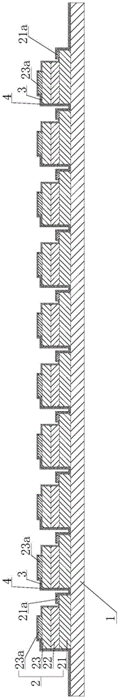
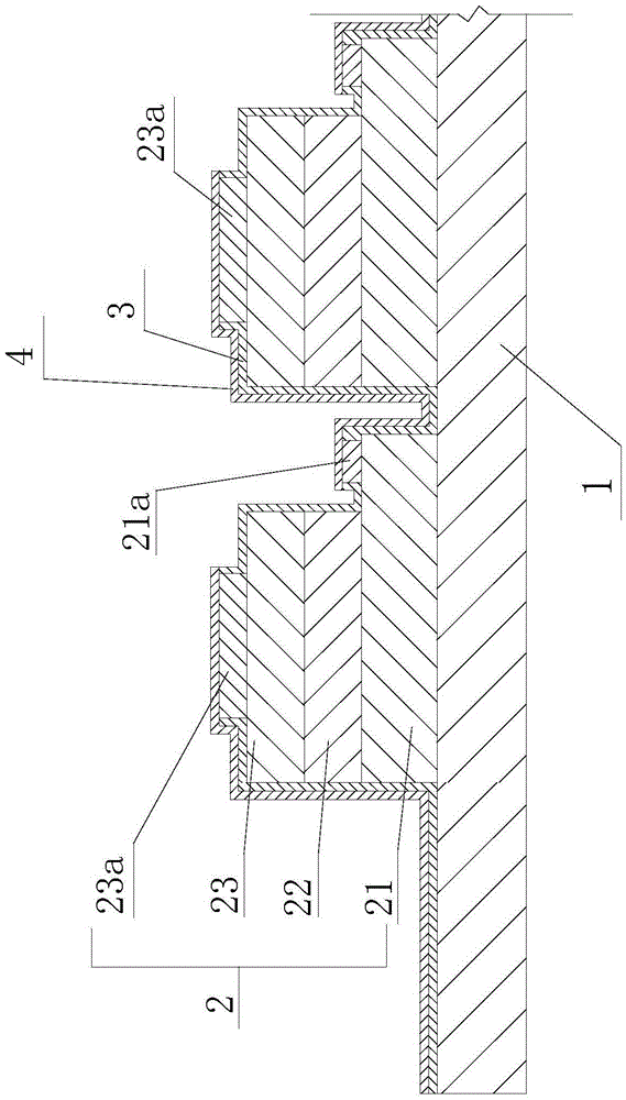
[0025] Such as Figure 1 to Figure 6 Shown: a filament of a three-dimensional light-emitting LED chip, including a strip-shaped transparent support 1 and a number of split diode light emitters 2 along the transparent support 1, the transparent support 1 constitutes the support of the whole chip, and the split diode light emitters 2 includes an N-GaN layer 21, an MQW light-emitting layer 22, and a P-GaN layer 23 stacked in sequence, an N electrode 21a is provided on the surface of the N-GaN layer 21, a P electrode 23a is provided on the surface of the P-GaN layer 23, and a P-electrode 23a is provided on the surface of the N electrode 21a and the surface of the split diode light emitter 2 at the P electrode 23a are provided with SiO 2 Passivation layer 3, on the upper surface of N electrode 21a and P electrode 23a on the opposite SiO 2 An exposed conduction window is formed at the passivation layer 3, SiO 2 The passivation layer 3 is covered with a metal circuit to connect the...


PUM

PropertyMeasurementUnit
widthaaaaaaaaaa

Abstract

The three-dimensional light-emitting LED chip filament of the present invention comprises a strip-shaped transparent support and several split diode light emitters are arranged along the transparent support, and its transparent support constitutes the support of the whole chip, and the split diode light emitters include sequentially stacked N-GaN layer, MQW light-emitting layer, P-GaN layer, N-electrodes are provided on the surface of the N-GaN layer, P-electrodes are provided on the surface of the P-GaN layer, and the surface of the split diode light emitter at the N-electrode and the P-electrode is provided. There is a SiO2 passivation layer, and an open conduction window is formed on the upper surface of the N electrode and the P electrode at the opposite SiO2 passivation layer, and the SiO2 passivation layer is covered with a metal line to connect the outer layer so that the adjacent split diodes The N electrode and the P electrode between the illuminants are connected in series in sequence, and the two ends are the extension ends of the external electrodes of the N electrode and the P electrode. The circuit series process forms the three-dimensional light-emitting LED chip filament and its The application of LED bulbs enables effective conduction through the circuit series process while achieving good connection stability and heat conduction effects.

Description

technical field [0001] The invention relates to an LED light source, more specifically, to a filament of a three-dimensional light-emitting LED chip and an LED bulb. Background technique [0002] The heat of traditional LED bulbs relies on the circuit substrate to conduct to the aluminum metal lamp holder and contact with the outside air to conduct and dissipate the heat. The circuit substrate of the integrated split diode light emitter is connected to the metal lamp holder to achieve the effect of conduction and heat dissipation , but there is a potential safety hazard of electric leakage when the two fit together. At the same time, if you want to improve the heat dissipation effect, you need to increase the heat dissipation area of ​​the aluminum metal lamp holder. The heat dissipation effect of the aluminum metal lamp holder is limited by the limited volume of the lamp body, so it cannot be fully Meet the heat dissipation effect required by LEDs, especially high-power LED...

Claims


Application Information

Patent Timeline
Patent Type & Authority Patents(China)
IPC IPC(8): H01L33/48H01L33/62H01L33/64
CPCH01L25/0753H01L33/62H01L33/64H01L24/24H01L2924/12041H01L2224/24H01L2924/00H01L2924/00012
Inventor 欧南杰
Owner DONGGUAN QIJIA ELECTRONICS CO LTD
Why Eureka
Try Eureka