Wafer level module and its fabricating method

A manufacturing method and wafer-level technology, which is applied in semiconductor/solid-state device manufacturing, radiation control devices, televisions, etc., and can solve the problems of general products and methods that do not have appropriate structures and methods, dislocation between substrates, and fewer modules. , to achieve the effect of increasing productivity and cost-effectiveness, precise control of pattern size, and increasing the number of modules

Active Publication Date: 2011-04-06
HIMAX TECH LTD
View PDF0 Cites 9 Cited by
  • Summary
  • Abstract
  • Description
  • Claims
  • Application Information

AI Technical Summary

Problems solved by technology

What's more, the movement of the liquid adhesive can cause misalignment between the substrates, resulting in a malfunctioning module
Therefore, traditional modules usually use larger safety margins when designing patterns, which will reduce the number of modules that can be manufactured on a single wafer
Also, it takes considerable time to apply or screen print liquid adhesives, especially complex patterns
[0003] Since the liquid adhesive cannot have a uniform thickness, wafer-level lens modules or camera modules usually need to use additional adjustment mechanisms, such as screws, to mechanically achieve the desired focal length, so the above-mentioned conventional wafer-level modules cannot be effectively designed and implemented. manufacture
[0004] It can be seen that the above-mentioned existing wafer-level modules and their manufacturing methods obviously still have inconveniences and defects in product structure, manufacturing method and use, and need to be further improved urgently.
In order to solve the above-mentioned problems, the relevant manufacturers have tried their best to find a solution, but no suitable design has been developed for a long time, and there is no suitable structure and method for general products and methods to solve the above-mentioned problems. This is obviously a problem that relevant industry players are eager to solve

Method used


Image

  • Wafer level module and its fabricating method
  • Wafer level module and its fabricating method
  • Wafer level module and its fabricating method

Examples


Embodiment Construction

[0041] In order to further explain the technical means and effects of the present invention to achieve the intended purpose of the invention, the specific implementation, structure, The method, steps, features and effects thereof are described in detail below.

[0042]The aforementioned and other technical contents, features and effects of the present invention will be clearly presented in the following detailed description of preferred embodiments with reference to the drawings. Through the description of the specific implementation mode, a more in-depth and specific understanding of the technical means and effects adopted by the present invention to achieve the intended purpose can be obtained. However, the accompanying drawings are only for reference and description, and are not used to explain the present invention. be restricted.

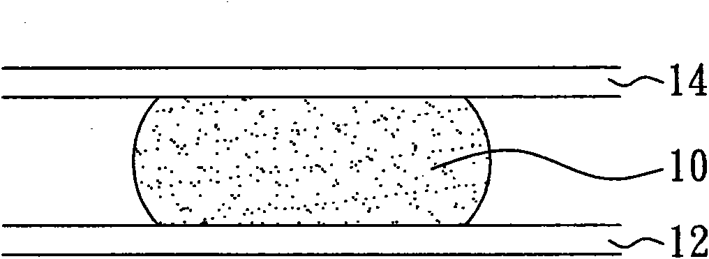
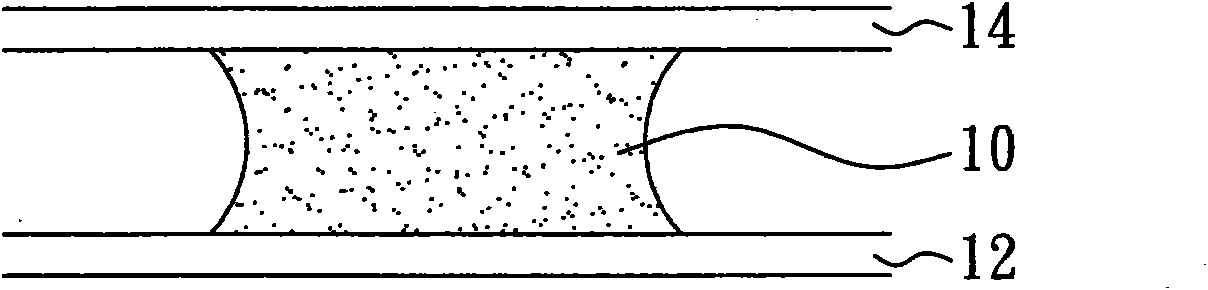
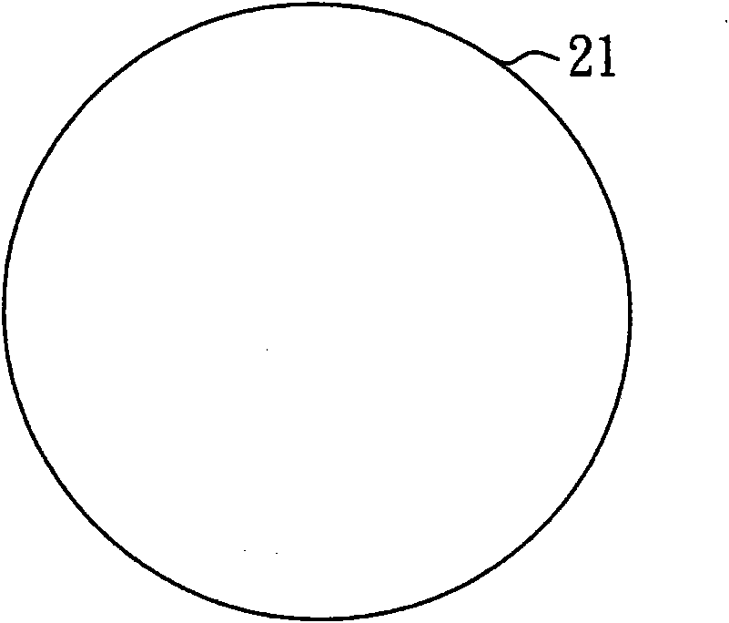
[0043] Figure 2A to Figure 2F is a schematic diagram of the structure of the wafer-level module and its manufacturing method according to t...


PUM


Abstract

The invention relates to a wafer level module and its fabricating method. The method of fabricating the wafer level module, comprises: providing a first solid adhesive film with a first release film and a second release film that respectively cover a first surface and a second surface of the first solid adhesive film; patterning a plurality of openings through the first solid adhesive film; removing the first release film to expose the first surface of the first solid adhesive film; and aligning and adhering the exposed first surface of the first solid adhesive film to a first substrate. The wafer level module is capable of effectively maintaining thickness evenness of the adhesive layer, and facilitating ease of alignment and application of the adhesive layer.

Description

technical field [0001] The invention relates to a wafer-level module, in particular to a structure of a wafer-level module with a solid adhesive film and a manufacturing method thereof. Background technique [0002] Wafer level optical technology uses semiconductor manufacturing processes to manufacture wafer-level small optical devices, such as lens modules or camera modules. This wafer-level optical technology is applicable to mobile or handheld electronic devices. In the manufacture of conventional WLOCs, usually screen printing or coating methods are used to bond two substrates with liquid adhesives. However, the characteristics of the liquid adhesive make it impossible to control the thickness of the formed adhesive layer and keep it constant. Furthermore, if Figure 1A and Figure 1B As shown, the liquid adhesive 10 between the substrate 12 and the substrate 14 may overflow. What's more, the movement of the liquid adhesive can cause misalignment between the substra...

Claims


Application Information

Patent Timeline
Patent Type & Authority Applications(China)
IPC IPC(8): H01L21/50H01L27/146H04N5/225
Inventor 熊信昌谈智伟苏柏霖
Owner HIMAX TECH LTD
Why Eureka
Try Eureka