
Chemical mechanical grinding method for interlayer dielectric layer

An interlayer dielectric layer and chemical-mechanical technology, which can be used in grinding devices, grinding machine tools, polishing compositions containing abrasives, etc., can solve problems such as affecting the yield of wafers

Inactive Publication Date: 2011-02-02
SEMICON MFG INT (SHANGHAI) CORP
View PDF0 Cites 7 Cited by
  • Summary
  • Abstract
  • Description
  • Claims
  • Application Information

AI Technical Summary

Problems solved by technology

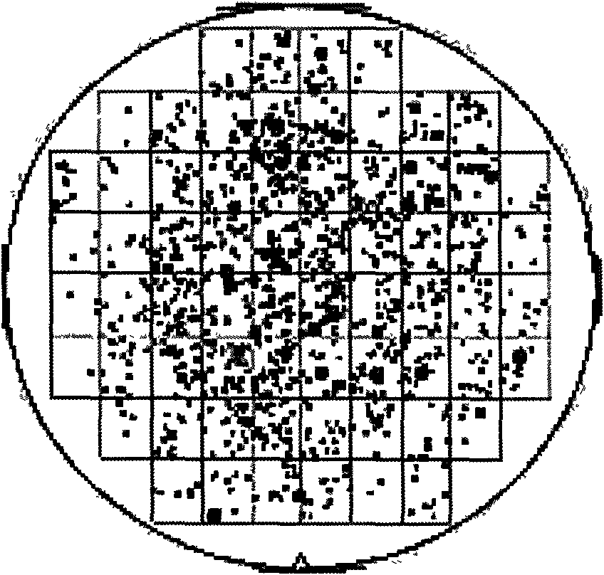
The number and size of scratches will seriously affect the yield of the wafer

Method used


Image

  • Chemical mechanical grinding method for interlayer dielectric layer
  • Chemical mechanical grinding method for interlayer dielectric layer
  • Chemical mechanical grinding method for interlayer dielectric layer

Examples


Embodiment Construction

[0017] In order to make the purpose, technical solution and advantages of the present invention clearer, the present invention will be further elaborated below in conjunction with the accompanying drawings.

[0018] The invention provides a chemical mechanical polishing method for an interlayer dielectric layer, referring to the attached image 3 The process flow chart shown includes: step S1, placing the wafer on the first polishing pad, and grinding the interlayer dielectric layer of the wafer, wherein the pressure between the first polishing pad and the wafer is 0.8-1.8 PSI, where 1psi≈6894.76Pa, preferably, the pressure between the first polishing pad and the wafer is 1.5PSI.

[0019] In this step, the grinding rate of the interlayer dielectric layer is 500-1200 Angstrom / minute, and the grinding time is 30-50 seconds. The preferred milling rate is 1000 angstroms / minute and the milling time is 40 seconds.

[0020] Wherein, the grinding liquid should be selected according ...


PUM


Abstract

The invention relates to a chemical mechanical grinding method for an interlayer dielectric layer, which comprises the following steps of: 1. grinding an interlayer dielectric layer of a wafer on a first grinding pad, wherein pressure between the first grinding pad and the wafer is 0.8-1.8PSI; 2. grinding the interlayer dielectric layer of the wafer on a second grinding pad, wherein pressure between the second grinding pad and the wafer is 0.8-1.8PSI, and most materials to be ground are removed in the first and second chemical mechanical grinding steps; and 3. grinding the interlayer dielectric layer of the wafer on a third grinding pad so as to further improve surface flat degree, wherein pressure between the third grinding pad and the wafer is 2.0-3.0PSI. The method can effectively reduce chemical mechanical grinding scratches of the interlayer dielectric layer and improve product yield.

Description

technical field [0001] The invention relates to a chemical-mechanical polishing (CMP) method, in particular to a method for chemical-mechanical polishing of an interlayer dielectric layer. Background technique [0002] The chemical mechanical polishing (CMP) process is to use mechanical force to act on the surface of the wafer in the atmospheric environment of the clean room to generate fracture corrosion power on the surface film layer, so that the surface of the wafer tends to be flattened, so that Subsequent process steps (such as photolithography) are performed. And this part must rely on the chemical substances in the polishing liquid to increase its etching efficiency by reacting. The two most important components in the CMP process are slurry and platen. The grinding liquid is usually made by dispersing some very fine oxide powder particles in an aqueous solution. Polishing pads are mostly made of foamed porous polyurethane. In the CMP process, the polishing liqui...

Claims


Application Information

Patent Timeline
IPC IPC(8): C09G1/02B24B37/04H01L21/304B24B37/02
Inventor 李健刘俊良
Owner SEMICON MFG INT (SHANGHAI) CORP
Learn More