Ramp wave output circuit, analog/digital conversion circuit, and camera
A technology of output circuit and output voltage, applied in the direction of delayed output pulse operation, electrical components, pulse processing, etc., can solve the problem of increasing the scale of the circuit, and achieve the effect of preventing the decline of the dynamic range
- Summary
- Abstract
- Description
- Claims
- Application Information
AI Technical Summary
Problems solved by technology
Method used
Image

Examples
no. 1 Embodiment approach
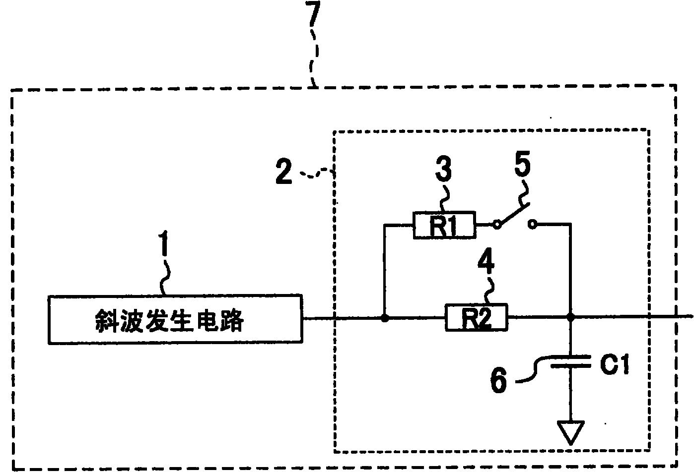
[0054] figure 1 The circuit configuration of the ramp output circuit according to the first embodiment of the present invention is shown.
[0055] Such as figure 1 As shown, the ramp wave output circuit 7 of this embodiment includes a ramp wave generating circuit 1 and a low-pass filter 2 having a variable characteristic function.
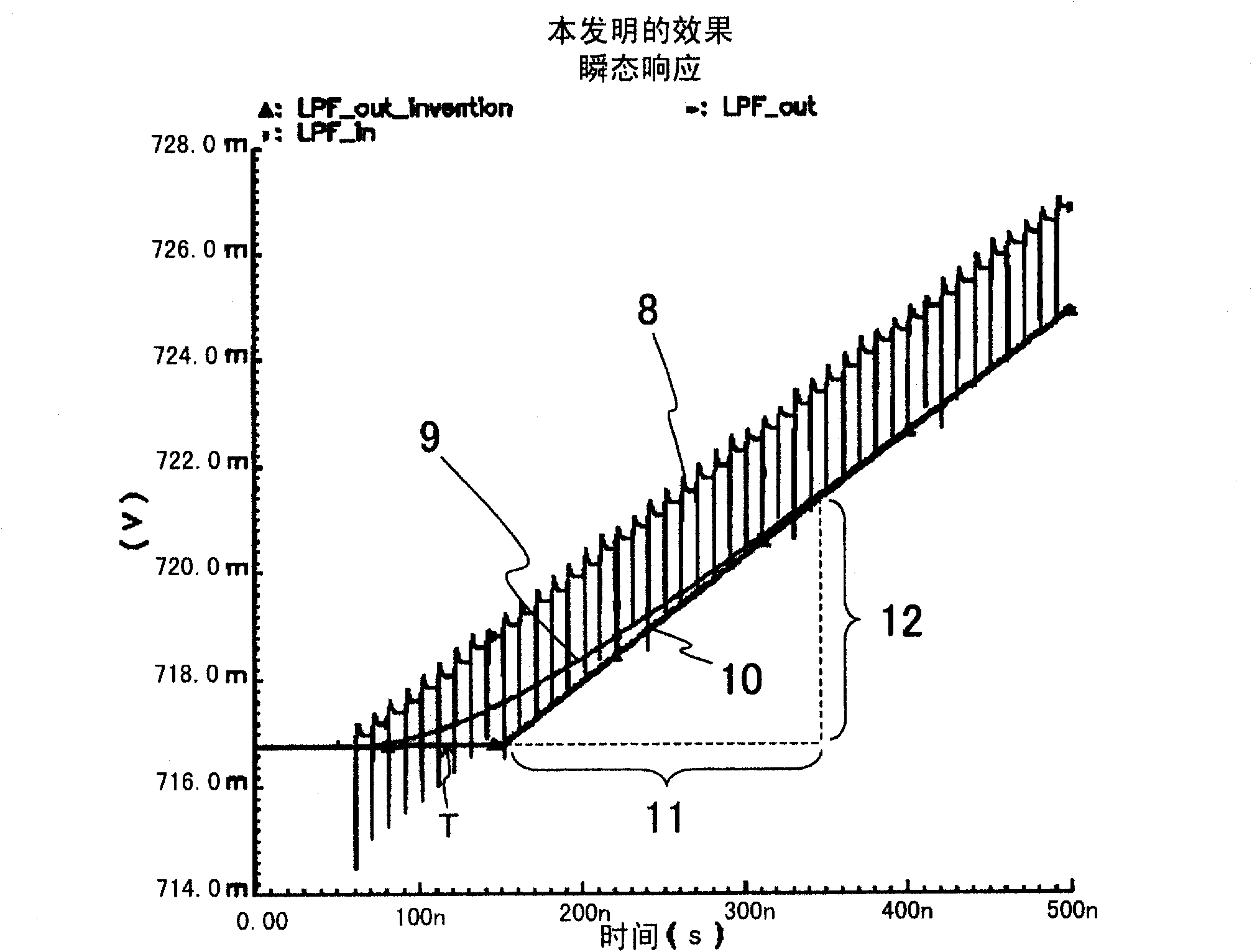
[0056] The low-pass filter 2 of this embodiment is a low-pass filter with a variable cutoff frequency, and performs filtering processing at a first cutoff frequency during a period from when the ramp wave output by the ramp wave generating circuit 1 is received to a predetermined time T. Then, after a predetermined time T has elapsed, filtering is performed at a second cutoff frequency having a frequency higher than the first cutoff frequency. In addition, the specific circuit structure of the low-pass filter 2 is such as this figure 1 and later described Figure 3 ~ Figure 5 shown in .
[0057] figure 1 The shown low-pass filter 2 is a prima...
Deformed example 1
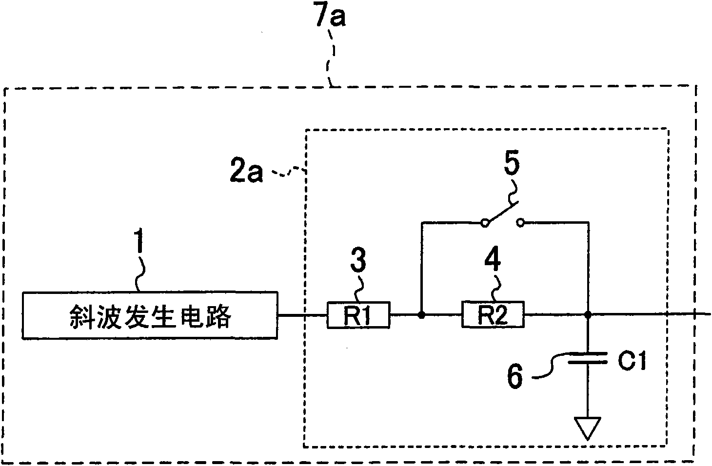
[0062] image 3 A circuit configuration including the low-pass filter 2 a of Modification 1 and the ramp output circuit 7 a of the aforementioned ramp generating circuit 1 is shown.
[0063] Such as image 3 As shown, the low-pass filter 2a of Modification 1 is a primary low-pass filter with a switchable resistance value structure, including: a resistor 3, a resistor 4, a switch 5, and a capacitor 6, for example, a resistor 3 with a resistance value R1 It is connected in series with a resistor 4 having a resistance value R2 sufficiently larger than the resistance value R1, the resistor 4 is connected in parallel with a switch 5, and one end of a capacitor 6 having a capacitance value C1 is connected to the resistor 4 and the switch 5.
[0064] The ramp wave output circuit 7a having the above structure is the same as when having the structure of the above-mentioned low-pass filter 2, and the switch 5 is turned off before the ramp wave from the ramp wave generating circuit 1 st...
Deformed example 2
[0066] Figure 4 A circuit configuration including the low-pass filter 2b according to Modification 2 and the ramp output circuit 7b of the aforementioned ramp generating circuit 1 is shown.
[0067] Such as Figure 4 As shown, the low-pass filter 2b of this modification 2 is a primary low-pass filter with a structure of switching capacitance, and has: a resistor 3, a switch 5, a capacitor 6, and a capacitor 13, for example, a capacitor 6 with a capacitance value C1 It is connected in series with a capacitor 13 having a capacitance value C2 that is sufficiently larger than the capacitance value C1, and the capacitor 6 is connected in parallel with the switch 5. One end of the resistor 3 having a resistance value R1 is connected to the ramp wave generating circuit 1, and the other end is connected to the capacitor 13. .
[0068] In the ramp wave output circuit 7b having the above configuration, the switch 5 is turned on from before the ramp wave generation from the ramp wave ...
PUM
 Abstract
Description
Claims
Application Information
 - R&D
- Intellectual Property
- Life Sciences
- Materials
- Tech Scout
- Unparalleled Data Quality
- Higher Quality Content
- 60% Fewer Hallucinations
Browse by: Latest US Patents, China's latest patents, Technical Efficacy Thesaurus, Application Domain, Technology Topic, Popular Technical Reports.
© 2025 PatSnap. All rights reserved.Legal|Privacy policy|Modern Slavery Act Transparency Statement|Sitemap|About US| Contact US: help@patsnap.com