Single-phase clock pass transistor adiabatic logic circuit, full adder and 5-2 compressor
A technology of adiabatic logic circuits and single-phase clocks, applied in logic circuits using specific components, logic circuits using semiconductor devices, etc. Small complexity, simple and standardized circuit structure, and the effect of reducing the area
- Summary
- Abstract
- Description
- Claims
- Application Information
AI Technical Summary
Problems solved by technology
Method used
Image
Examples
Embodiment 1
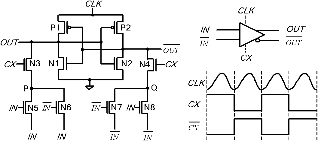
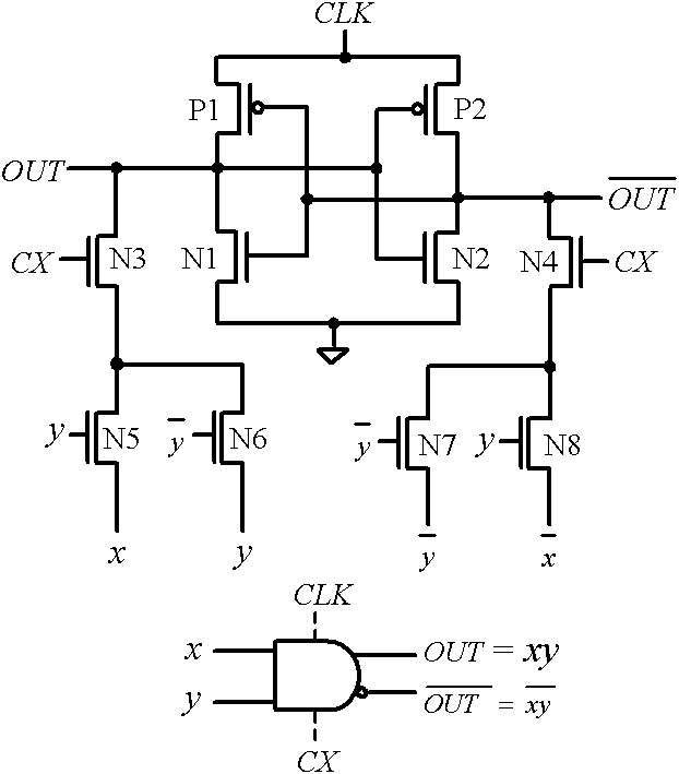
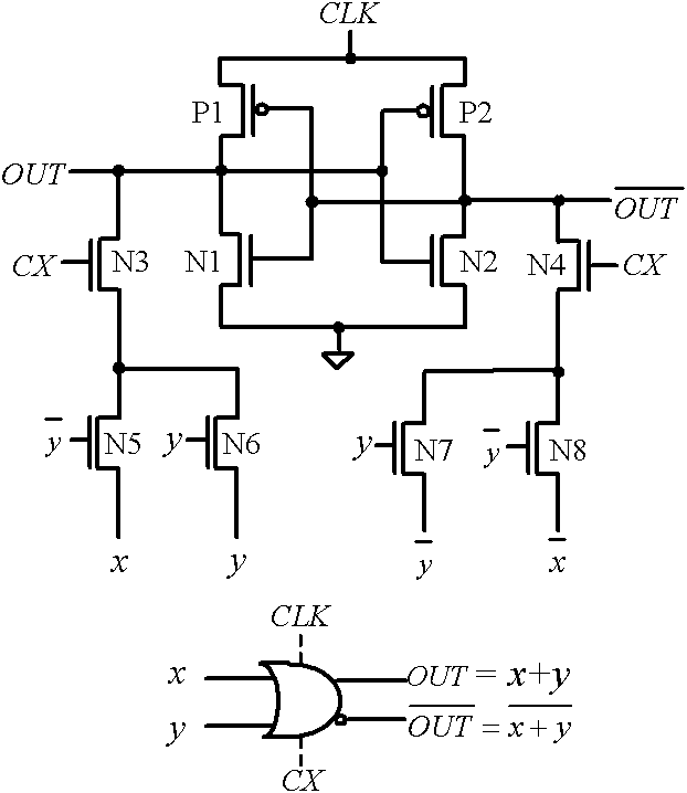
[0027] Embodiment one: if figure 1 As shown, the single-phase clock transmission tube adiabatic logic circuit is composed of a logic evaluation circuit and an energy recovery circuit, wherein the energy recovery circuit is composed of the first pMOS transistor P1 and the second pMOS transistor P2, and the clamp is composed of the first nMOS transistor N1 and the second pMOS transistor. Two nMOS transistors N2 are used to prevent the output node from being suspended. CX is an auxiliary clock signal introduced to control the input signal. It is controlled by the third nMOS transistor N3 and the fourth nMOS transistor N4. The first pMOS transistor P1 and The source of the second pMOS transistor P2 is connected to the power clock terminal CLK, the substrate is connected to the high level, the drain of the first pMOS transistor P1 is connected to the source of the first nMOS transistor N1, and the source of the second pMOS transistor P2 The drain is connected to the source of the s...
Embodiment 2
[0029] Embodiment two: the symbol figure of the single-phase adiabatic full adder of the present invention is as Figure 5 As shown, A, B, C i are the three adder input ports of the full adder, CLK is the power clock terminal, CX is the auxiliary clock signal terminal, C is the carry signal output terminal of the full adder, S is the sum signal output terminal of the full adder, it is It consists of a carry signal generation circuit and a summation signal generation circuit. The carry signal generation circuit is shown in Figure 6(a), which consists of the first single-phase clock transmission tube adiabatic logic circuit and 8 nMOS tubes, that is, the ninth nMOS tube N9, the The tenth nMOS transistor N10, the eleventh nMOS transistor N11, the twelfth nMOS transistor N12, the thirteenth nMOS transistor N13, the fourteenth nMOS transistor N14, the fifteenth nMOS transistor N15 and the sixteenth nMOS transistor N16, the first The single-phase clock transmission tube adiabatic l...
Embodiment 3
[0031] Embodiment Three: The structure of the single-phase adiabatic 5-2 compressor of the present invention is as follows Figure 10 As shown, its basic principle is to add 7 numbers (five actual input data I1, I2, I3, I4, I5, two carry inputs Cin1, Cin2) to generate 4 numbers Sum, Carry, Cout1, Cout2 output , where the carry Cout1, Cout2 will not be passed to the next stage, but as the input signal Cin1, Cin2 of the adjacent high bit, so as to realize the 5-2 compression function. It is formed by cascading the first full adder I, the second full adder II and the third full adder III, the first adder input terminal A1 of the first full adder I is connected to the first input signal I1, The second addend input terminal B1 of the first full adder I is connected with the second input signal I2, and the third addend input terminal C of the first full adder I i 1 is connected with the third input signal I3, the carry signal output terminal C1 of the first full adder I outputs the...
PUM
 Abstract
Description
Claims
Application Information
 - R&D
- Intellectual Property
- Life Sciences
- Materials
- Tech Scout
- Unparalleled Data Quality
- Higher Quality Content
- 60% Fewer Hallucinations
Browse by: Latest US Patents, China's latest patents, Technical Efficacy Thesaurus, Application Domain, Technology Topic, Popular Technical Reports.
© 2025 PatSnap. All rights reserved.Legal|Privacy policy|Modern Slavery Act Transparency Statement|Sitemap|About US| Contact US: help@patsnap.com


