
Chip card assembly and disassembly structure of electronic device

A technology of electronic devices and chip cards, which is applied to the parts of connecting devices, coupling devices, circuits, etc., can solve the problems of inconvenient operation for users and large space of electronic devices, and achieve the effects of saving volume, convenient taking out, and simple structure

Inactive Publication Date: 2010-12-29
SHENZHEN FUTAIHONG PRECISION IND CO LTD +1
View PDF0 Cites 0 Cited by
  • Summary
  • Abstract
  • Description
  • Claims
  • Application Information

AI Technical Summary

Problems solved by technology

[0004] However, this kind of chip card loading and unloading structure takes up a lot of space in the electronic device, and when taking out the chip card, the battery cover needs to be opened first, and the chip card can only be taken out after taking out the battery, which brings great inconvenience to the user.

Method used


Image

  • Chip card assembly and disassembly structure of electronic device
  • Chip card assembly and disassembly structure of electronic device
  • Chip card assembly and disassembly structure of electronic device

Examples


Embodiment Construction

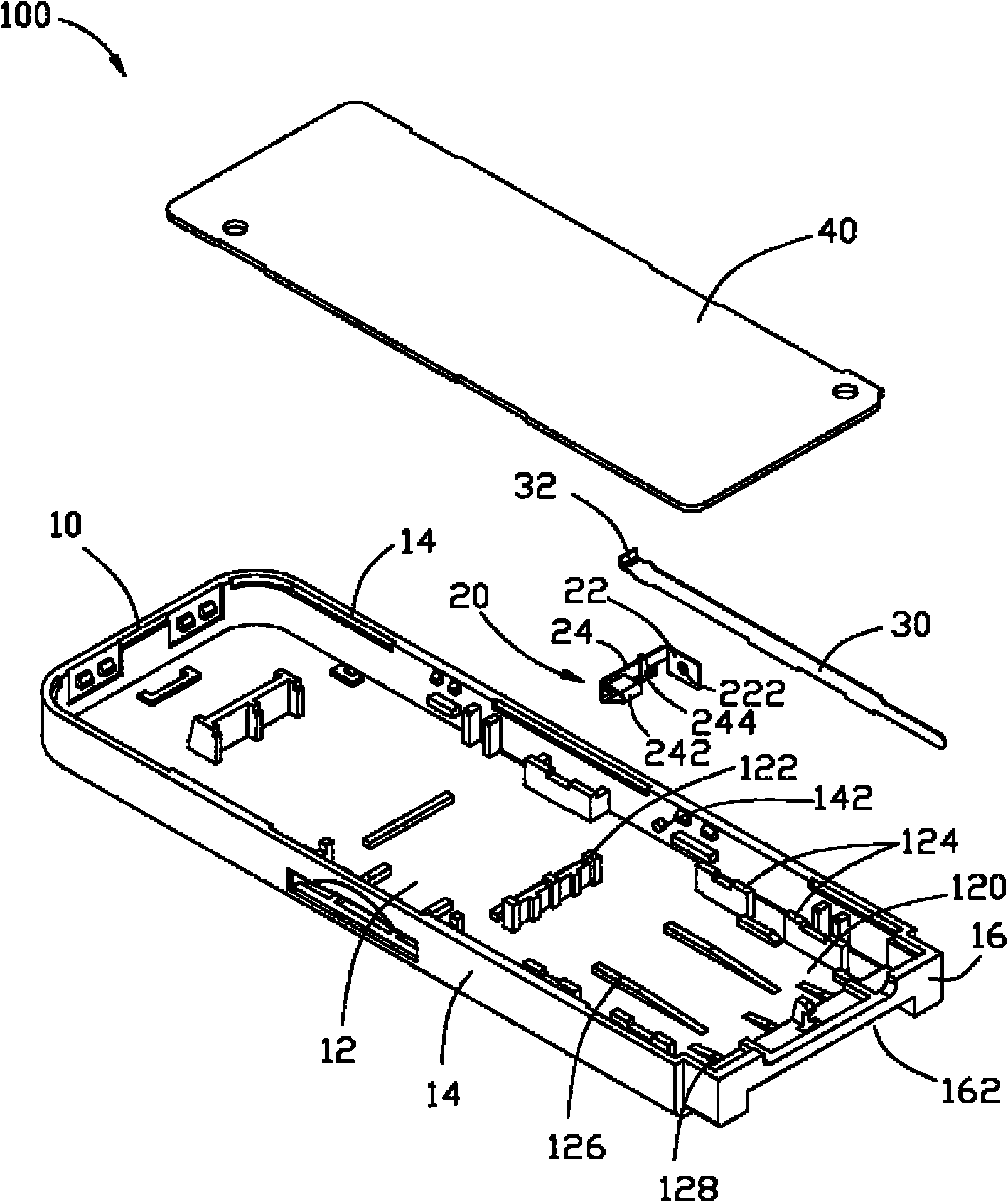
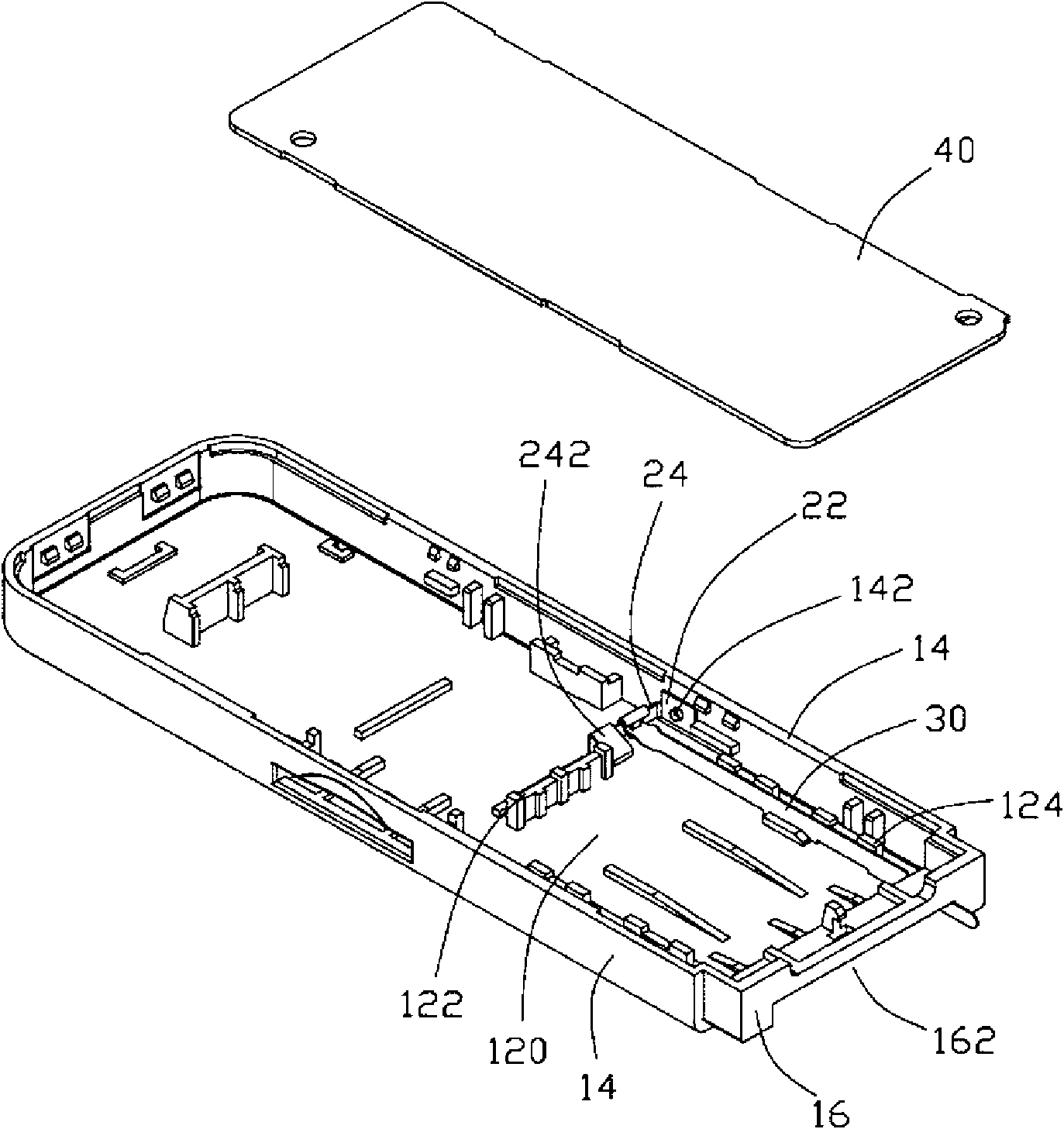
[0011] see figure 1 According to a preferred embodiment of the present invention, a chip card loading and unloading structure 100 of an electronic device includes a housing 10 , an elastic member 20 , a stretching member 30 and a circuit board 40 .

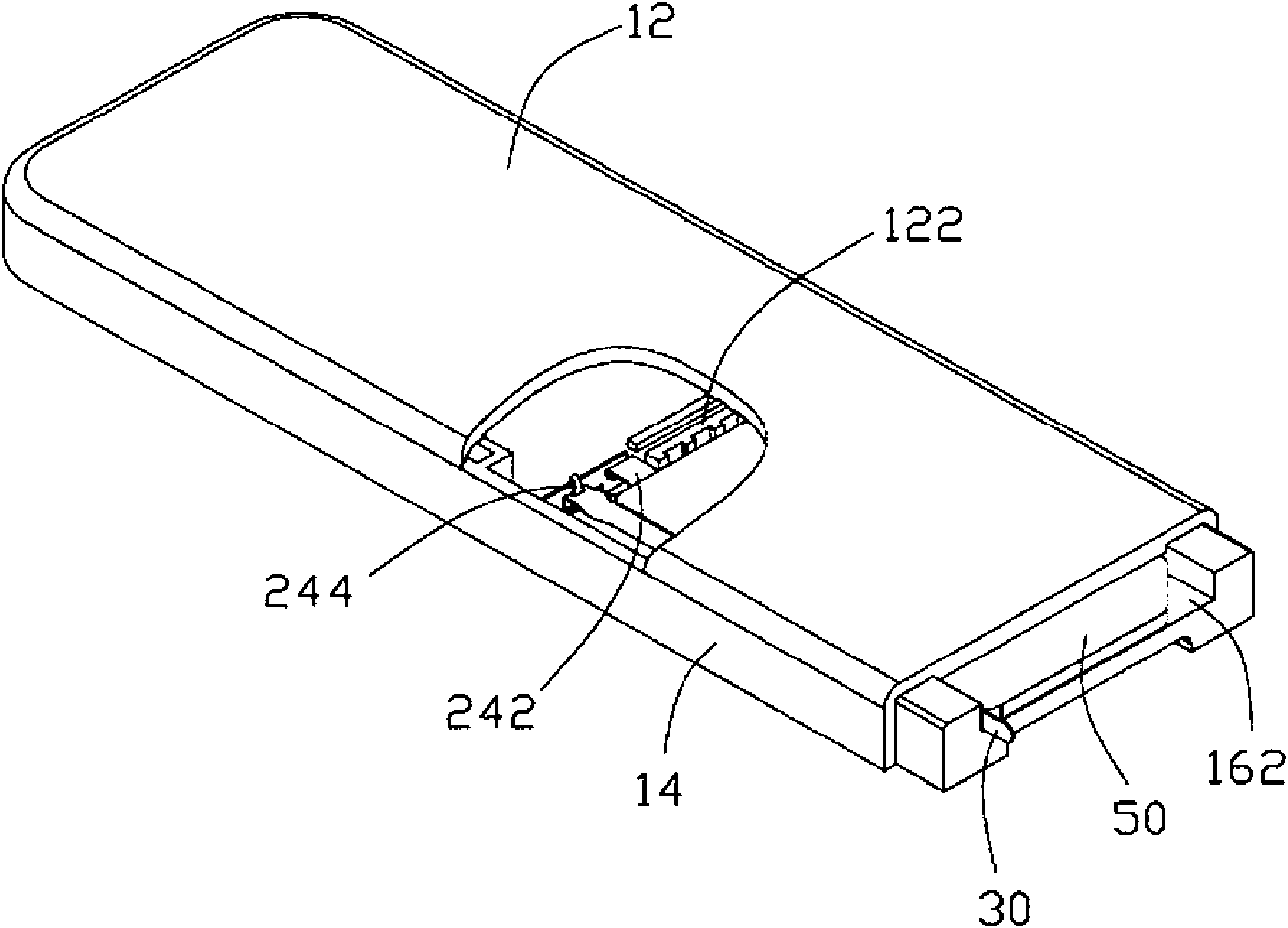
[0012] The casing 10 is a rectangular frame structure, which includes a bottom wall 12 , two side walls 14 and an end wall 16 mounted on the outer periphery of the bottom wall 12 . A stopper wall 122 and a plurality of fixed walls 124 protrude from the bottom wall 12 . The stop wall 122 is parallel to the end wall 16 , the distance between it and the end wall 16 is slightly larger than the length of a chip card, and forms a certain distance from the two side walls 14 . The fixing walls 124 are parallel to the side walls 14 , are symmetrically arranged in two groups and adjacent to the side walls 14 respectively. The bottom wall 12 , the stop wall 122 , the fixing wall 124 and the end wall 16 enclose a receiving frame 120 for rec...


PUM


Abstract

The invention discloses a chip card assembly and disassembly structure of an electronic device. The structure comprises a shell, an elastic part, a stretching part and a circuit board, wherein the shell comprises a bottom wall and an end wall; the bottom wall is provided with an accommodating frame for accommodating a chip card; the end wall is provided with an opening which is communicated with the accommodating frame; the elastic part is fixedly connected to one end on the shell corresponding to the opening; one end of the stretching part is connected to the elastic part, while the other end stretches out of the opening; the circuit board is arranged on the shell and covers the accommodating frame; the chip card is inserted into the opening to be arranged; and the elastic part is pressed against the chip card to make the chip card withdrawn from the opening by pulling the stretching part. The chip card assembly and disassembly structure has the advantages of simpleness, small occupied space of the electronic device, and contribution to the assembly and withdrawal of the chip card.

Description

technical field [0001] The invention relates to a chip card loading and unloading structure of an electronic device. Background technique [0002] In recent years, surface connection cards with integrated circuits are widely used in electronic devices to improve or expand the functions of electronic devices, such as SIM cards installed in mobile phones, which store information data such as user's personal information and several phone numbers. Therefore, the mobile phone also needs to be provided with a loading and unloading structure for installing the chip card. [0003] The loading and unloading structure of the common chip card in the industry is usually arranged on the back casing of the electronic device, and is located at the bottom of the battery storage frame. It opens a chip card storage slot on the casing, and forms two sides of the storage slot on the storage slot. Connected one-card holder. When loading the chip card, insert the chip card obliquely from one en...

Claims


Application Information

Patent Timeline
Patent Type & Authority Applications(China)
IPC IPC(8): H01R13/629H01R13/635H01R12/22H01R12/71
CPCG06K13/08Y10S439/946Y10S439/945
Inventor 张正龙
Owner SHENZHEN FUTAIHONG PRECISION IND CO LTD
Learn More