Electrostatic chuck and plasma device

A technology of electrostatic adsorption and plasma, applied in the direction of circuits, discharge tubes, electrical components, etc., can solve problems such as difficult repairs, gas leakage, etc., and achieve the effects of reducing SCCM, reducing dissipation, and extending economic benefits

Inactive Publication Date: 2010-12-29
TAIWAN SEMICON MFG CO LTD
View PDF0 Cites 12 Cited by
  • Summary
  • Abstract
  • Description
  • Claims
  • Application Information

AI Technical Summary

Problems solved by technology

Using epoxy in these areas can slow down the damage of the ESC pad, but epoxy is not resistant to wear from plasma and plasma by-products, so gas leaks and edge arcing will continue to occur
Additionally, the use of epoxy on the ESC is permanent, which can make repairing damaged epoxy or other components in the ESC difficult

Method used


Image

  • Electrostatic chuck and plasma device
  • Electrostatic chuck and plasma device
  • Electrostatic chuck and plasma device

Examples


Embodiment Construction

[0033] The present invention will be described in the specification with respect to various embodiments in particular, that is, with respect to the use of an electrostatic adsorption chuck (ESC) in a plasma chamber. The present invention can also be applied to other forms of electrostatic adsorption trays and other forms of technology.

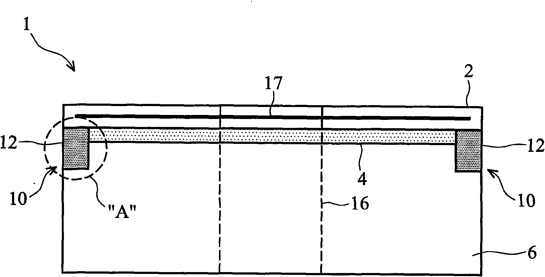
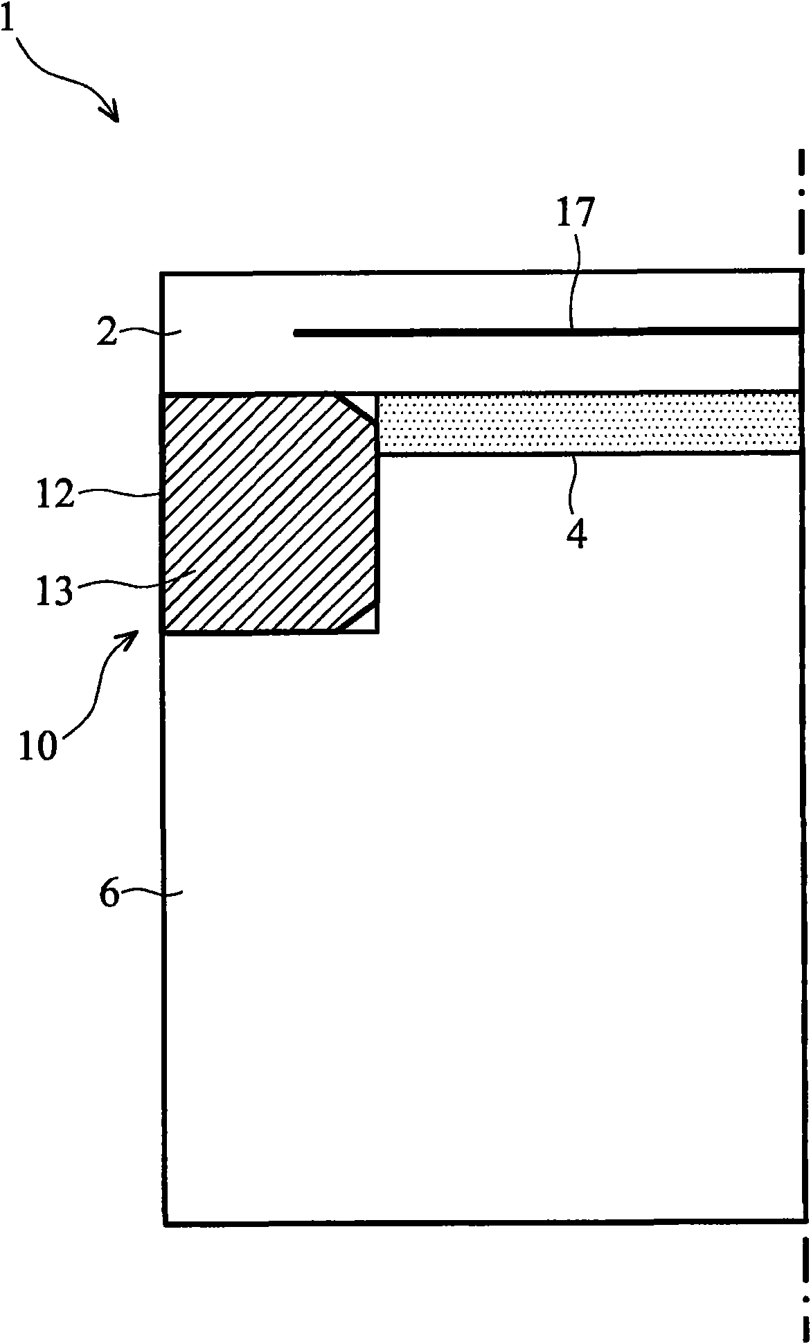
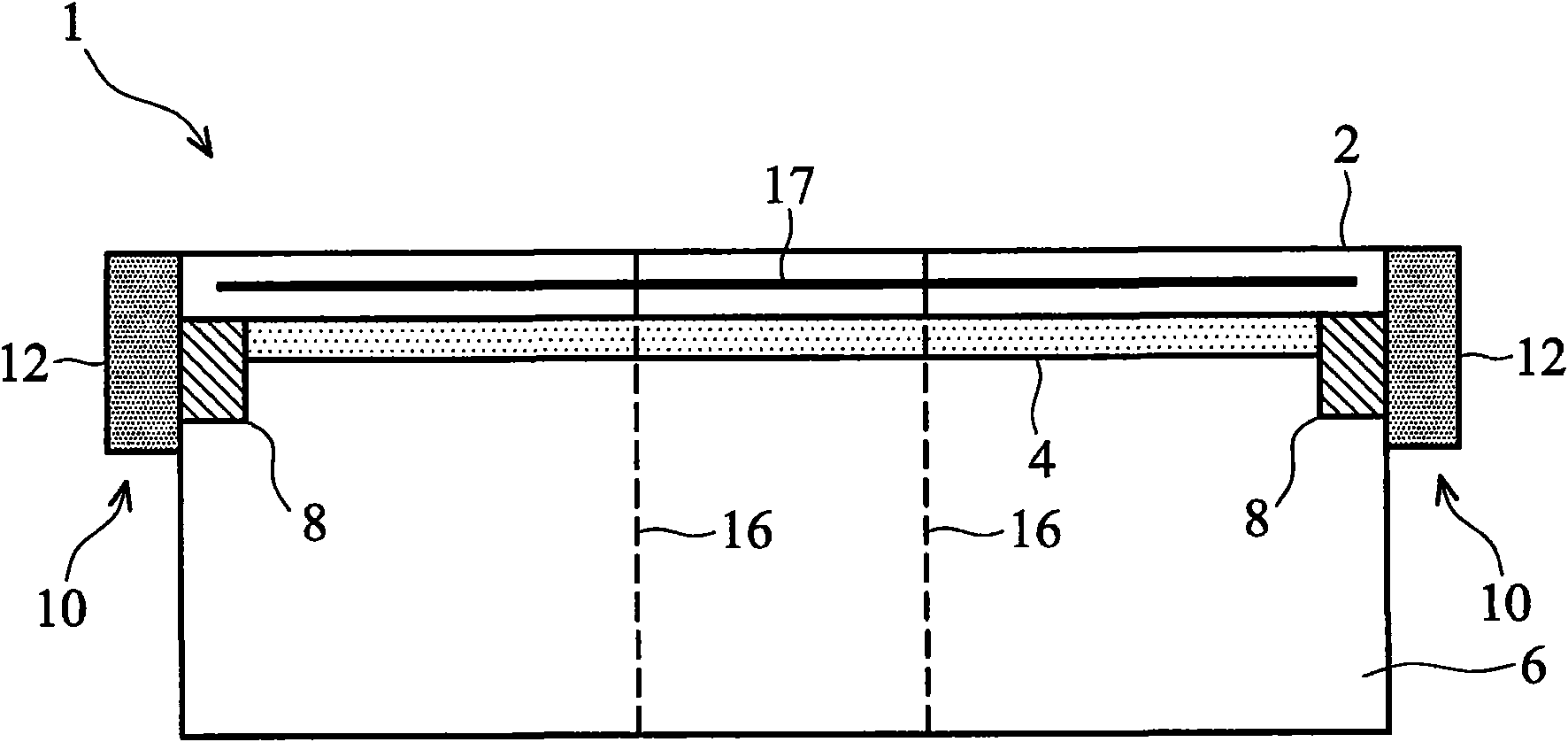
[0034] Now see the illustration, Figure 1A to Figure 1D Shown is the cross-sectional area of ​​an electrostatic adsorption chuck (ESC) 1 . Such as Figure 1A In the illustrated embodiment, the ESC 1 includes an upper element 2 , a bonding layer 4 , a lower element 6 , a notch 10 , a replaceable sidewall shield 12 , an air hole 16 and a conductive electrode 17 .

[0035] The conductive electrode 17 includes a conductive material, such as tungsten, for receiving voltage and serving as an electrode. Lower member 6 receives heat transfer gas through vents 16 to transfer heat from the wafer (not shown) during the process. In this embodiment, t...


PUM


Abstract

The invention provides an electrostatic chuck and a plasma device. The electrostatic chuck has a base member, a top member residing on a top surface of the base member, an indentation located at the interface of the base member and the top member, and a replaceable sidewall shield. The replaceable sidewall shield fills an indentation located between a base member and a top member of an electrostatic chuck, such that the replaceable electrostatic chuck sidewall shield may protect an epoxy in the indentation or may replace the epoxy within the indentation. The replaceable electrostatic chuck sidewall shield may be fully contained with the indentation. The replaceable electrostatic chuck sidewall shield may also cover an epoxy in the indentation such that the replaceable electrostatic chuck sidewall shield protrudes beyond the indentation. In an alternate embodiment, the replaceable electrostatic chuck sidewall shield substantially covers the area in which a conductive pole is embedded in a bipolar electrostatic chuck.

Description

technical field [0001] The invention relates to a manufacturing device of an integrated circuit, in particular to an electrostatic adsorption holding plate device with a sealed side wall. Background technique [0002] In today's semiconductor integrated circuit process, etching is a process used to pattern circuits on semiconductors. Plasma etching is a type of etching process in which a high-speed stream of ions is directed at a wafer. The ions etch the wafer surface, thereby modifying the physical topography and patterning of the wafer. A plasma etching device generally includes a plasma chamber and an electrostatic chuck (ESC) in the plasma chamber. [0003] An electrostatic chuck (ESC) is a device that uses electricity to generate electrostatic forces, such as Coulomb force and Johnson-Rahbek force, which are used to hold a wafer in a plasma chamber during wafer processing. position in . ESCs generally consist of a lower element as an electrode, an upper element cons...

Claims


Application Information

Patent Timeline
Patent Type & Authority Applications(China)
IPC IPC(8): H01J37/20H01J37/32H01L21/02
CPCH01L21/6833
Inventor 刘旭水汪业杰白峻荣
Owner TAIWAN SEMICON MFG CO LTD
Why Eureka
Try Eureka