Method for welding inner conductor of filter and PCB and cavity filter
A cavity filter, PCB board technology, used in waveguide-type devices, welding/welding connections, electrical components, etc., can solve the problems of high product defect rate and difficult to reach products, so as to reduce product defect rate and improve production efficiency. , the effect of reducing production costs
- Summary
- Abstract
- Description
- Claims
- Application Information
AI Technical Summary
Problems solved by technology
Method used
Image

Examples
Embodiment 1
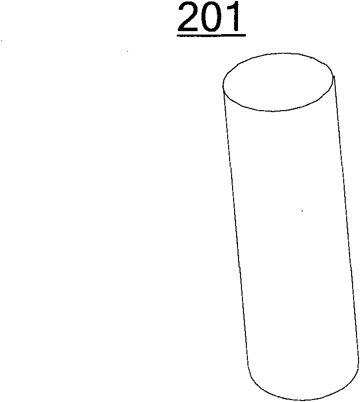
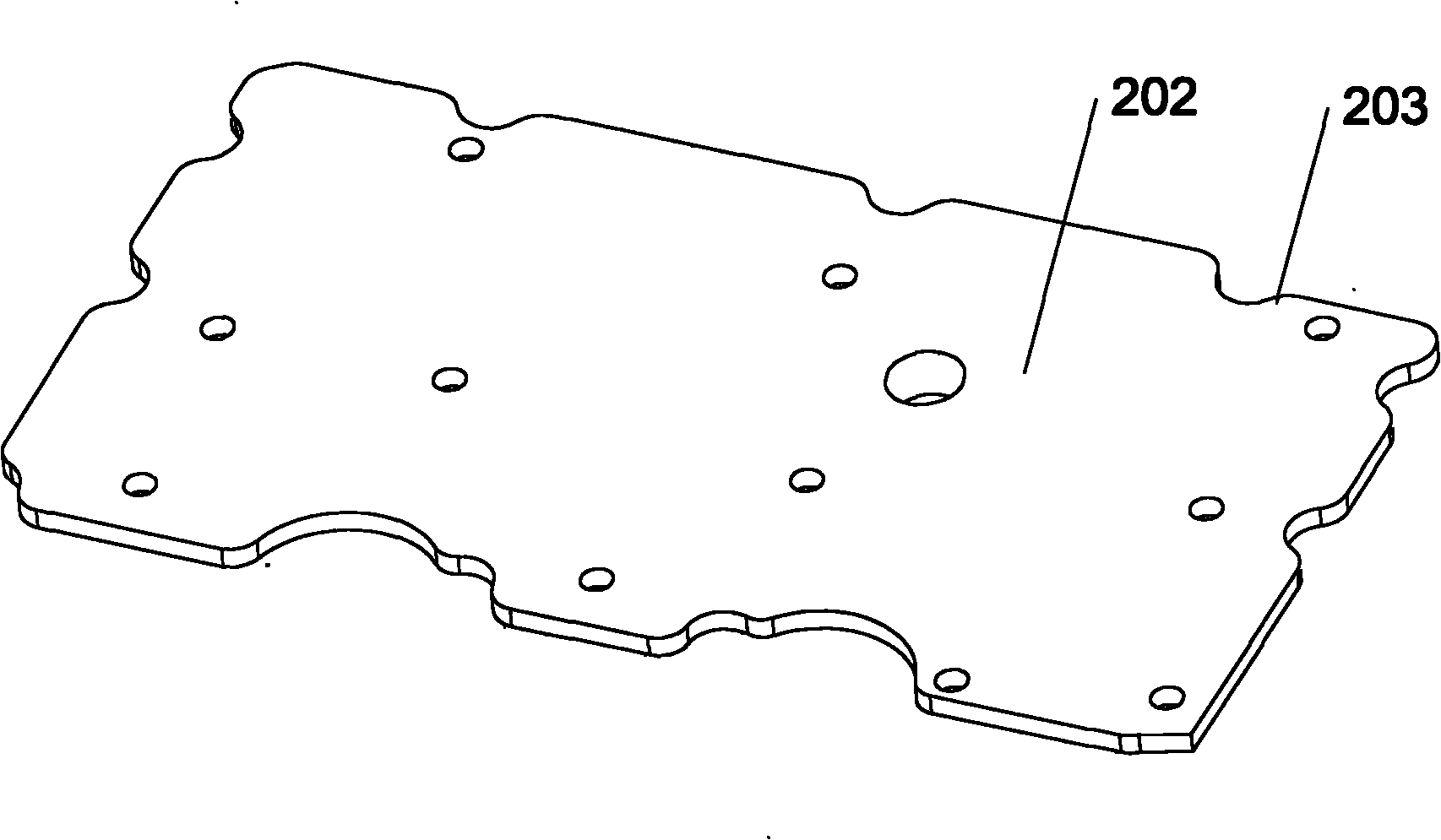
[0029] Embodiment 1. A welding method for the inner conductor of a filter and a PCB board. Referring to FIG. 2(a) and FIG. Hole 202, including:
[0030] A1, insert the inner conductor 201 into the connection hole 202 on the PCB board 203;
[0031] In this embodiment, an inner conductor is provided. As shown in FIG. The structure can require multiple deformations according to the design of the filter, and its specific implementation does not constitute a limitation to the present invention; a PCB board with connection holes is provided, as shown in Figure 2 (b); the inner conductor 201 is inserted into the PCB The connecting hole 202 on the board 203, as shown in Fig. 2(c) and Fig. 2(d), can be realized by using a designed jig, other tools or manually. The size of the connection hole 202 on the PCB is adapted to the size of the inner conductor 201 .
[0032] A2, as shown in Figure 2(d), adjust the position of the inner conductor so that the distance between the top surface 2...
Embodiment 2
[0047] Embodiment 2, a welding method for the inner conductor of a filter and a PCB board, referring to Fig. 4(a) and Fig. 4(b) together, the PCB board 403 is provided with a connection suitable for the inner conductor 401 Hole 402, including:
[0048] A1, insert the inner conductor 401 into the connection hole 402 on the PCB 403;
[0049] In this embodiment, an inner conductor 401 is provided, including an inner conductor body 441 and an inner conductor connection end 442, as shown in FIG. 4(a); a PCB board 403 with a connection hole 402 is provided, as shown in FIG. As shown in b); Insert the inner conductor 401 into the connection hole 402 of the PCB board 403, as shown in Figure 4(c) and Figure 4(d), it can be realized by using a designed jig, other tools or manually. The size of the connection hole 402 on the PCB is adapted to the size of the inner conductor 401 .
[0050] A2, referring to FIG. 4(e), adjust the position of the inner conductor 401 so that the distance be...
Embodiment 3
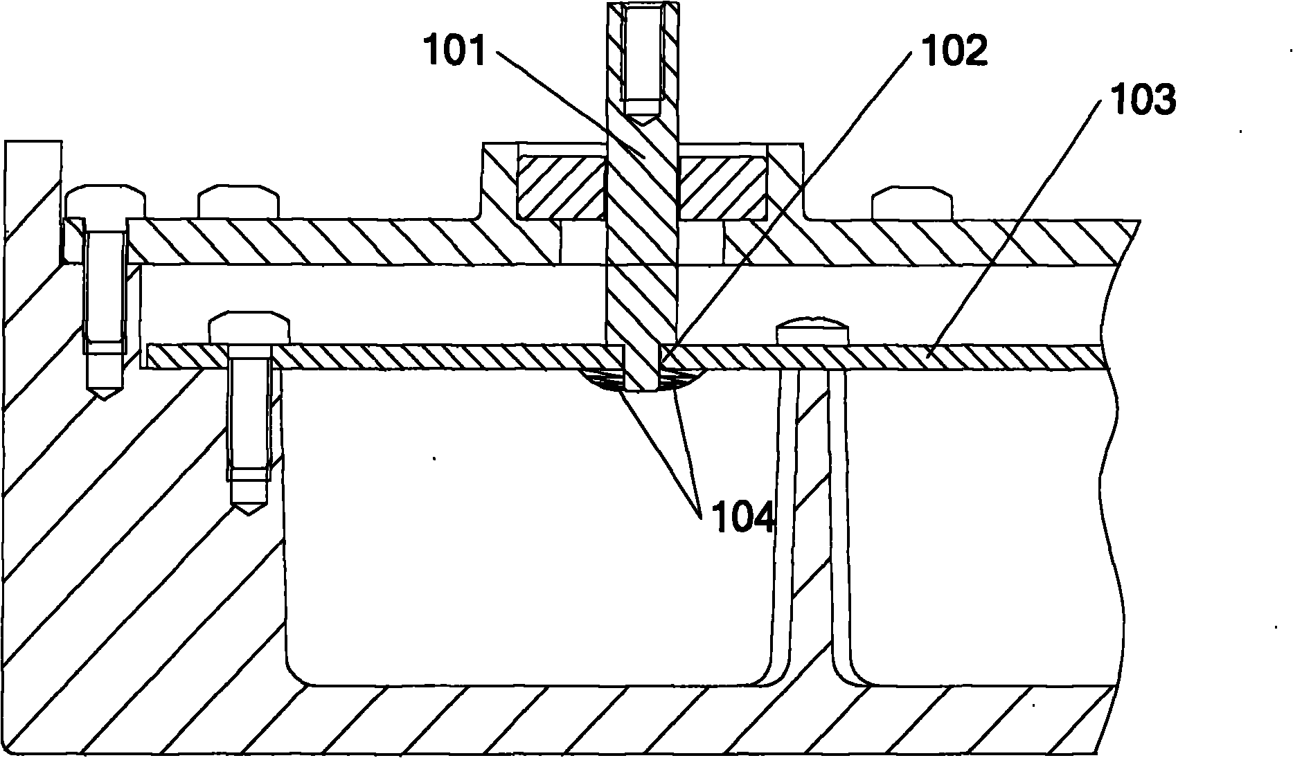
[0069] Embodiment 3. A cavity filter, including a cavity, a cover plate, an inner conductor 701, and a PCB board 703. The PCB board has a connection hole for inserting the inner conductor, and the position of the inner conductor 701 is according to The distance between the top surface 712 of the inner conductor and the bottom surface 713 of the PCB is determined.
[0070] The PCB board includes an upper surface 720 of the PCB board and a lower surface 713 of the PCB board, and the inner conductor 701 is inserted into a connection hole from the upper surface 720 of the PCB board, passes out from the lower surface 713 of the PCB board, and passes through the lower surface 713 of the PCB board. position, at least one of the upper surface of the PCB board and the lower surface of the PCB board is welded to the inner conductor to form a welding portion 731 and / or a welding portion 732 . It can be understood that if there is a gap between the inner conductor and the PCB board at the...
PUM
 Abstract
Description
Claims
Application Information
 - R&D
- Intellectual Property
- Life Sciences
- Materials
- Tech Scout
- Unparalleled Data Quality
- Higher Quality Content
- 60% Fewer Hallucinations
Browse by: Latest US Patents, China's latest patents, Technical Efficacy Thesaurus, Application Domain, Technology Topic, Popular Technical Reports.
© 2025 PatSnap. All rights reserved.Legal|Privacy policy|Modern Slavery Act Transparency Statement|Sitemap|About US| Contact US: help@patsnap.com