Novel plate crimped dual-chip encapsulated ceramic package

A flat crimping, ceramic shell technology, applied in electrical components, electrical solid devices, circuits, etc., to achieve the effect of increasing the heat dissipation area, high insulation, and improving the ability to resist thermal fatigue

Inactive Publication Date: 2010-12-15
江阴市赛英电子股份有限公司
View PDF0 Cites 4 Cited by
  • Summary
  • Abstract
  • Description
  • Claims
  • Application Information

AI Technical Summary

Problems solved by technology

At present, the module packaging method using high-performance plastic shells can already realize the combined packaging of multiple chips, but due to the influence of many factors such as withstand voltage, sealing, and heat dissipation, the module packaging is generally only suitable for applications in the small and medium power field. It has become one of the main directions in the industry to make a flat ceramic structure with high insulation, high strength and high sealing to realize the composition and packaging of two or more chips.

Method used


Image

  • Novel plate crimped dual-chip encapsulated ceramic package
  • Novel plate crimped dual-chip encapsulated ceramic package
  • Novel plate crimped dual-chip encapsulated ceramic package

Examples


Embodiment Construction

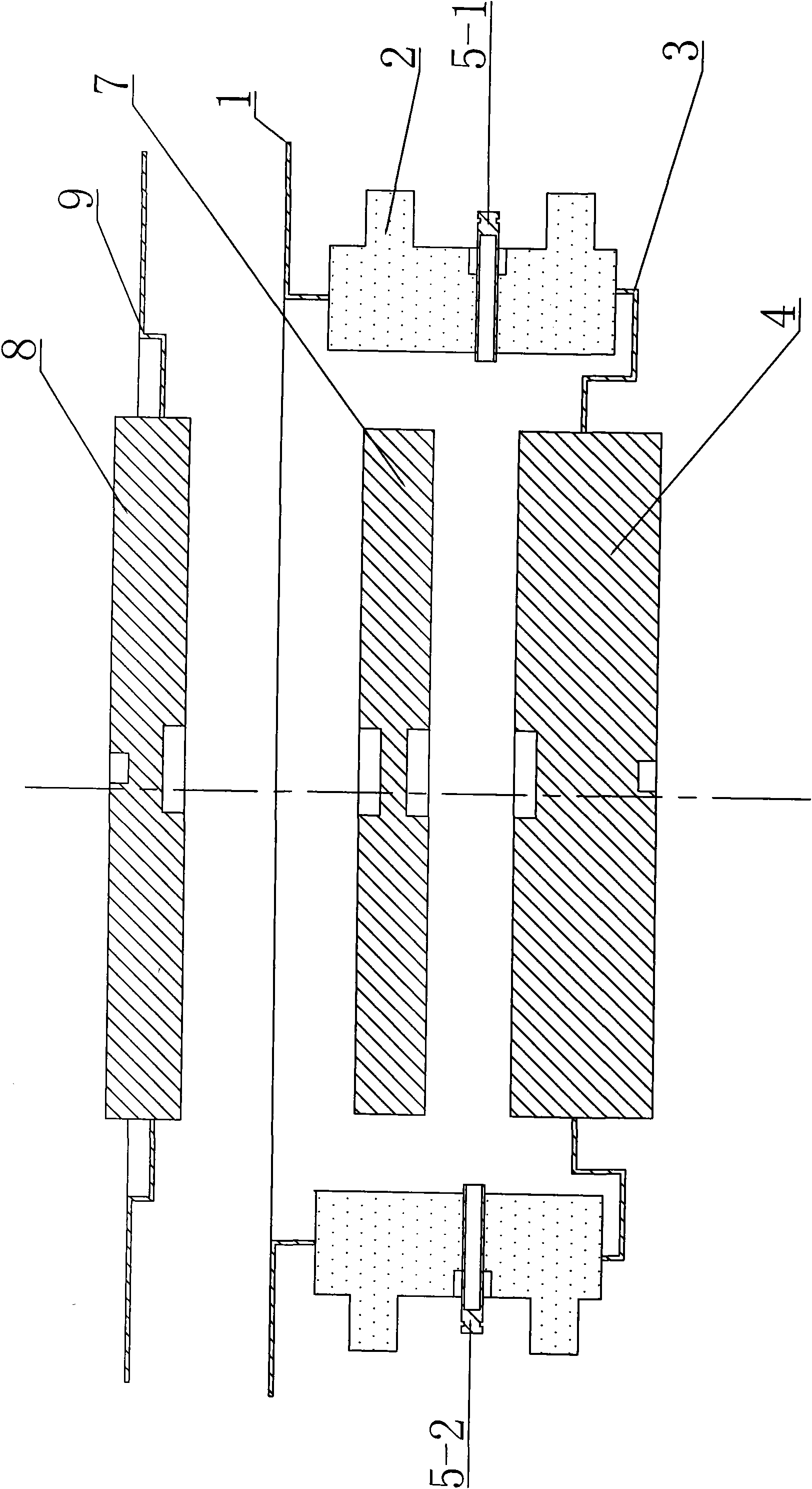
[0024] see figure 1 , the present invention relates to a novel flat crimping double-chip packaging ceramic case, which consists of three parts: a ceramic base, a transition electrode 7 and an upper cover;

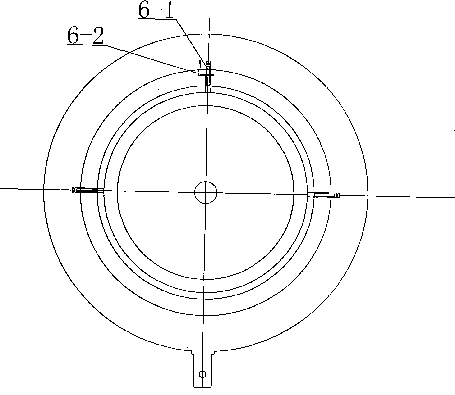
[0025] see Figure 1~2 , the ceramic base is mainly composed of an anode flange 1, a ceramic ring 2, an anode sealing ring 3, an anode electrode 4, a gate lead tube 1 5-1, a gate lead tube 2 5-2, a cathode lead tube 6-1, Composed of cathode inserts 6-2, the inner edge of the anode sealing ring 3 is concentrically welded to the outer edge of the anode electrode 4, the outer edge is concentrically welded to the lower end surface of the ceramic ring 2, and the anode flange 1 is concentrically welded to the upper end surface of the ceramic ring 2, The anode flange 1, the ceramic ring 2 and the anode sealing ring 3 are stacked and welded concentrically from top to bottom, and the first gate lead tube 5-1 and the second gate lead tube 5-2 are horizontally connected to the center...


PUM


Abstract

The invention relates to a novel plate crimped dual-chip encapsulated ceramic package, which consists of a ceramic base, a transition electrode (7) and an upper cover, wherein the ceramic base mainly comprises an anodic flange (1), a ceramic ring (2), an anodic sealing ring (3), an anodic electrode (4), a first gate fairlead (5-1), a second gate fairlead (5-2), a cathodic fairlead (6-1), and a cathodic insert (6-2); the transition electrode (7) is arranged between the ceramic base and the upper cover; and the upper cover mainly comprises a cathodic electrode (8) and a cathodic flange (9) which is concentrically welded on the other edge of the cathodic electrode (8). The new plate crimped dual-chip encapsulated ceramic package of the invention can realize serial encapsulation of two chips.

Description

(1) Technical field [0001] The invention relates to a novel ceramic shell, in particular to a crimping type ceramic shell capable of packing two chips in a single flat panel device, which belongs to the technical field of power electronics. (2) Background technology [0002] High-power semiconductor devices generally consist of chips, casings, and heat sinks. For flat-panel devices with ceramic structures, a single chip package is used, that is to say, only one chip is packaged in a device. The advantages of this single package method are simple structure, good heat dissipation effect, and low process requirements; The disadvantages are that the device is bulky, the consumables are high, and there are many external lines. Due to the restriction of the capacity of a single device, it is generally necessary to use multiple devices in series or parallel in actual use. For example, a 6-inch high-power semiconductor device with the largest specification at present, the capacity ...

Claims


Application Information

Patent Timeline
IPC IPC(8): H01L23/053H01L23/08
Inventor 陈国贤徐宏伟陈蓓璐
Owner 江阴市赛英电子股份有限公司
Why Eureka
Try Eureka