Structure of wide gain spectrum quantum dot material for semiconductor optical amplifier

A technology of quantum dot materials and optical amplifiers, applied to the structure of the active region, etc., can solve the problems of speed bottleneck and high system cost

Inactive Publication Date: 2012-07-04
INST OF SEMICONDUCTORS - CHINESE ACAD OF SCI
View PDF0 Cites 0 Cited by
  • Summary
  • Abstract
  • Description
  • Claims
  • Application Information

AI Technical Summary

Problems solved by technology

However, for the amplification and processing of multiple channels in the WDM system, it needs to be demultiplexed and then processed separately. On the one hand, the system cost is too high, and on the other hand, it leads to a speed bottleneck.

Method used


Image

  • Structure of wide gain spectrum quantum dot material for semiconductor optical amplifier
  • Structure of wide gain spectrum quantum dot material for semiconductor optical amplifier
  • Structure of wide gain spectrum quantum dot material for semiconductor optical amplifier

Examples


Embodiment Construction

[0035] In order to make the object, technical solution and advantages of the present invention clearer, the present invention will be described in further detail below in conjunction with specific embodiments and with reference to the accompanying drawings.

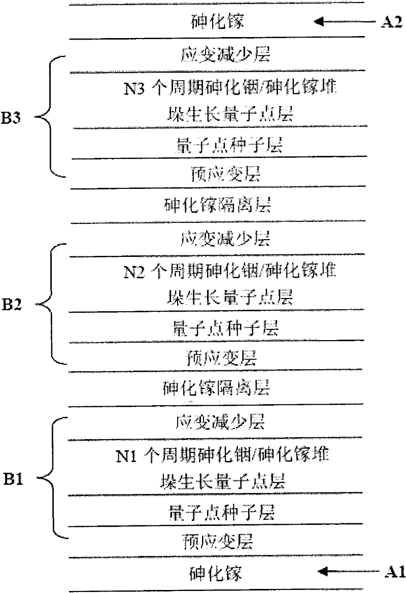
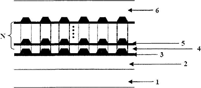
[0036] Please refer to the accompanying drawings, figure 1 It is a schematic diagram of a wide gain spectrum quantum dot material structure for a semiconductor optical amplifier provided by the present invention. The structure utilizes the non-uniform broadening characteristics of quantum dots designed with multiple layers of different sizes to obtain a wide gain spectrum, including:

[0037] An N-type gallium arsenide substrate 1;

[0038] An N-type gallium arsenide buffer layer 2, grown on the N-type gallium arsenide substrate 1 at a growth temperature of 600°C, for isolating defects on the substrate;

[0039] An N-type AlGaAs optical lower confinement layer 3, grown on the N-type GaAs buffer layer 2 at a growth temper...


PUM


Abstract

The invention discloses a structure of a wide gain spectrum quantum dot material for a semiconductor optical amplifier. The structure comprises an N-type gallium arsenide substrate, an N-type gallium arsenide buffer layer which grows on the N-type gallium arsenide substrate and is used for isolating defects on the substrate, an N-type gallium aluminum arsenide optical lower limiting layer which grows on the N-type gallium arsenide buffer layer and is used for limiting optical modes and current carriers, a self-organizing quantum dot active layer with multiple layers and different periods which grows on the N-type gallium aluminum arsenide optical lower limiting layer, a P-type gallium aluminum arsenide optical upper limiting layer which grows on the quantum dot active layer and is used for limiting the optical modes and current carriers, and a P-type gallium arsenide cap layer which grows on the P-type gallium aluminum arsenide optical upper limiting layer and is used for contacting an electrode. The wide gain spectrum is obtained by using inhomogeneous broadening characteristic of quantum dots with multiple layers and different sizes in the structure.

Description

technical field [0001] The invention relates to the technical field of semiconductor optoelectronic materials and devices, in particular to a wide gain spectrum quantum dot material structure used in semiconductor optical amplifiers. Background technique [0002] With the development of a new generation of large-capacity high-speed optical communication technology and all-optical network technology, wavelength division multiplexing system has become a key technology for optical signal transmission because it can maximize the use of optical fiber transmission capacity. However, the amplification and processing of multiple channels in the wavelength division multiplexing system need to be demultiplexed and then performed separately. On the one hand, the cost of the system is too high, and on the other hand, it causes a speed bottleneck. Using quantum dot materials to make semiconductor optical amplifiers can not only achieve simultaneous amplification and processing of multipl...

Claims


Application Information

Patent Timeline
Patent Type & Authority Patents(China)
IPC IPC(8): H01S5/30
Inventor 刘王来叶小玲徐波王占国
Owner INST OF SEMICONDUCTORS - CHINESE ACAD OF SCI
Why Eureka
Try Eureka