Insulated gate bipolar transistor
A technology of bipolar transistors and insulated gates, applied in semiconductor devices, electrical components, circuits, etc., can solve the problems of difficult hole discharge and reduction of the main unit area, and achieve the effect of suppressing the decrease of current density and improving the accumulation effect
- Summary
- Abstract
- Description
- Claims
- Application Information
AI Technical Summary
Problems solved by technology
Method used
Image
Examples
Embodiment 1
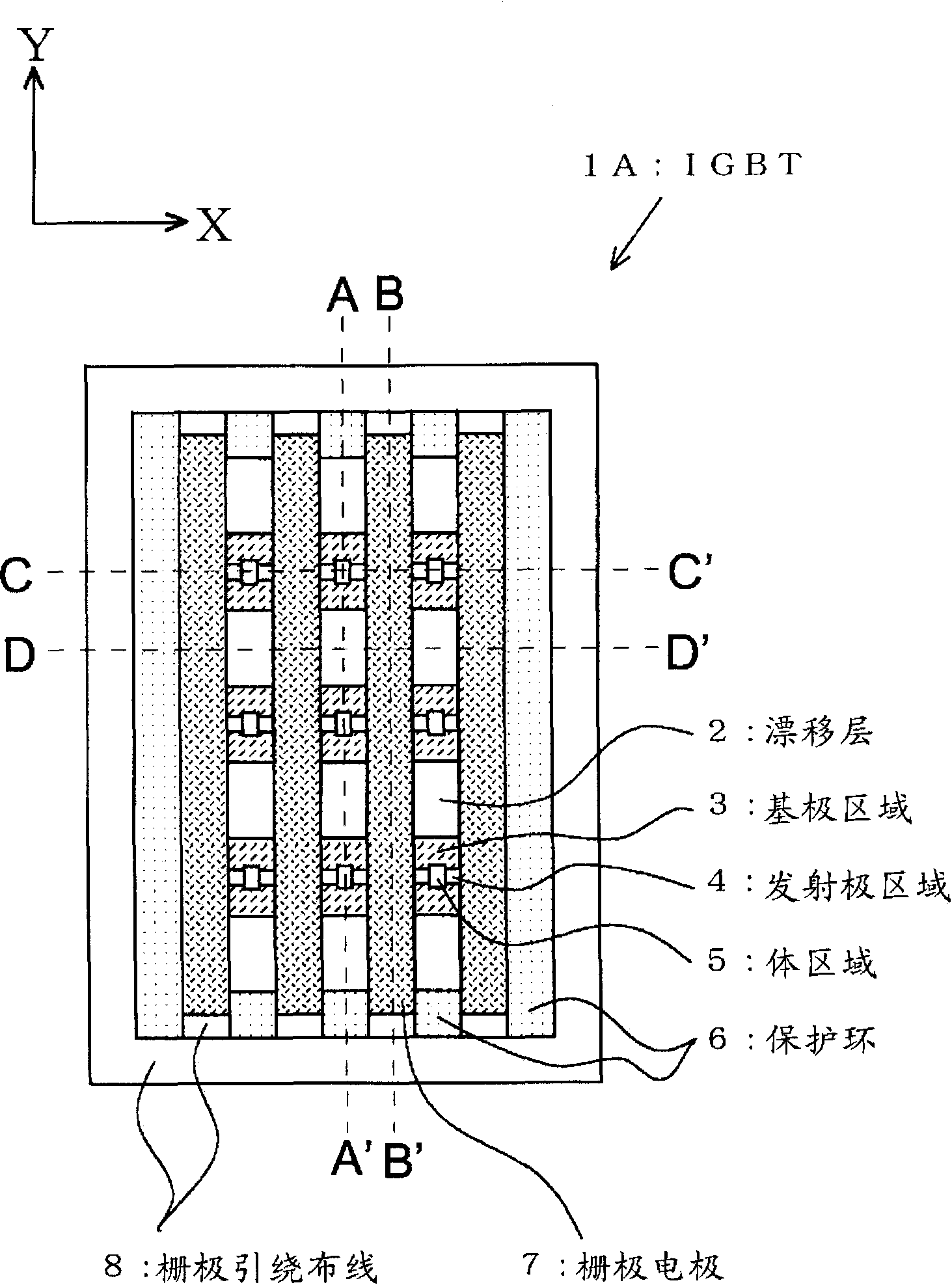
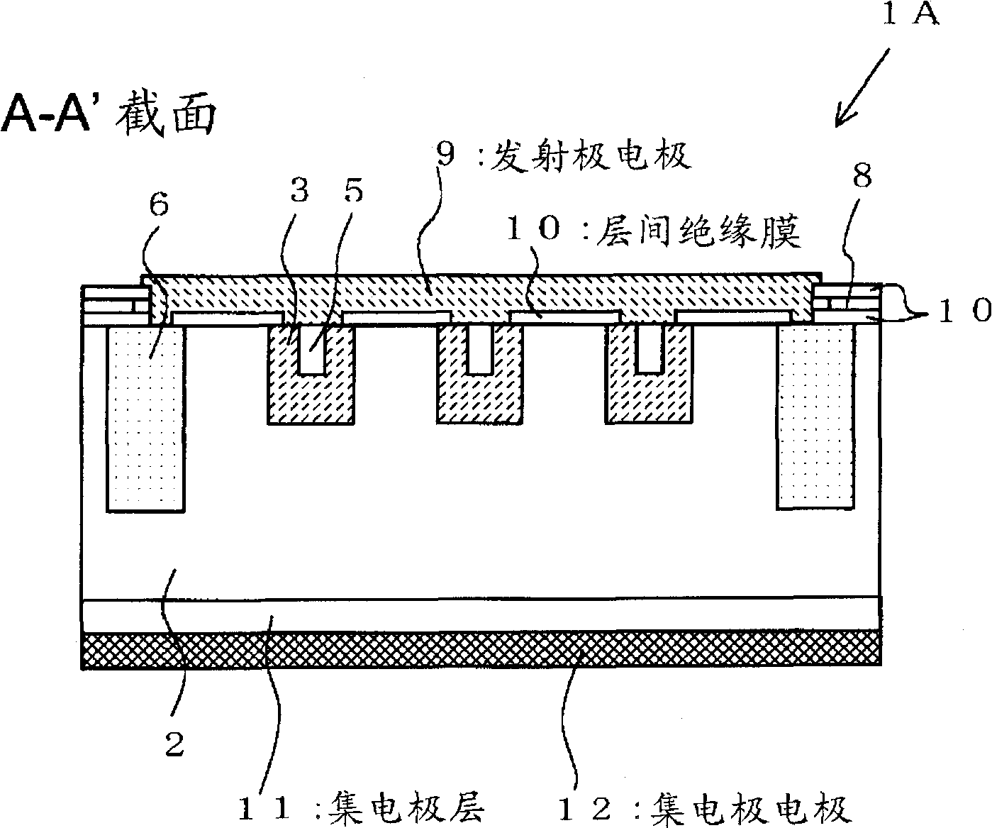
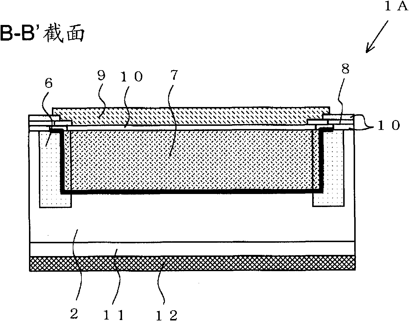
[0029] First, refer to Figure 1~5 The structure of IGBT 1A according to the first embodiment of the present invention will be specifically described. figure 1 is a top view of the IGBT. in addition, figure 2 , 3 , 4 and 5 are respectively figure 1 The cross-sectional view of the IGBT along the lines A-A', B-B', C-C', and D-D'.
[0030] First, refer to figure 1 The plan view structure of IGBT 1A according to the first embodiment will be described. IGBT 1A includes drift layer 2 , base region 3 , emitter region 4 , body region 5 , guard ring 6 , gate electrode 7 , and gate routing wiring 8 . In addition, the emitter electrode 9 connected to the emitter region 4 and the interlayer insulating film 10 insulating the emitter electrode 9 from the drift layer 2 or the gate electrode 7 are actually formed. Their illustrations are omitted in .
[0031] Each component will be described in detail. The gate electrode 7 has a stripe shape extending in the Y direction. Also, a ...
Embodiment 2
[0056] Next, the IGBT 1B according to the second embodiment will be described. In this IGBT 1B, the effect of accumulating holes is further improved compared with the IGBT 1A according to the first embodiment.
[0057] Figure 6 A cross section of IGBT 1B according to this embodiment along line A-A' corresponding to IGBT 1A according to First Embodiment is shown ( figure 2 ) of the cross-sectional structure.
[0058] In contrast to the first embodiment, in the IGBT 1B according to the present embodiment, the N-type conductivity type hole discharge suppression region 13 is formed on the side surface of the base region 3 . The other structures are the same as those of the first embodiment, and thus description thereof will be omitted here.
[0059] To describe the effect of this structure, when referring to the section along line A-A' of IGBT 1A related to the first embodiment ( figure 2 ), in the IGBT 1A according to the first embodiment, holes are reliably accumulated un...
PUM
 Abstract
Description
Claims
Application Information
 - R&D
- Intellectual Property
- Life Sciences
- Materials
- Tech Scout
- Unparalleled Data Quality
- Higher Quality Content
- 60% Fewer Hallucinations
Browse by: Latest US Patents, China's latest patents, Technical Efficacy Thesaurus, Application Domain, Technology Topic, Popular Technical Reports.
© 2025 PatSnap. All rights reserved.Legal|Privacy policy|Modern Slavery Act Transparency Statement|Sitemap|About US| Contact US: help@patsnap.com


