Iron-doped carbon thin-film material with photovoltaic and photoconductive effects and preparation method thereof
A thin-film material and photoconductive technology, applied in the direction of photovoltaic power generation, circuits, electrical components, etc., can solve the problems of further improvement in use and response range, high environmental protection requirements and safety requirements for the preparation process, and achieve stable process, superior performance, Inexpensive effect
- Summary
- Abstract
- Description
- Claims
- Application Information
AI Technical Summary
Problems solved by technology
Method used
Image
Examples
Embodiment 1
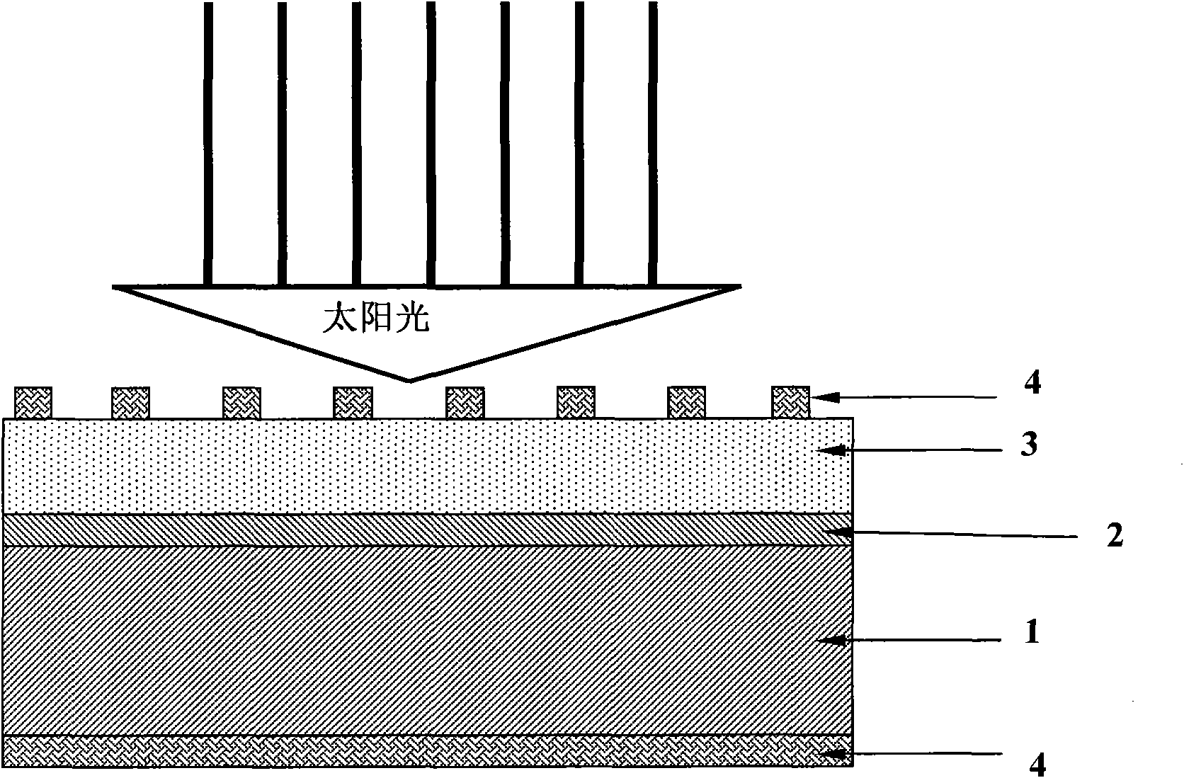
[0023] (a-C:Fe) / Al with Photovoltaic and Photoconductive Effects 2 o 3 / Si iron-doped carbon thin film material, on the n-type Si substrate 1, an aluminum oxide layer 2 and an iron-doped carbon layer 3 (a-C:Fe layer) are sequentially arranged to form an iron-doped carbon thin film material with photovoltaic and photoconductive effects .
[0024] The iron-doped carbon thin film material with photovoltaic and photoconductive effects is prepared by laser pulse deposition method. The steps of the method are as follows: n-type Si(100) substrate, Al 2 o 3 The single crystal target, Fe target and high-purity C target are placed in the vacuum coating chamber of the laser pulse deposition equipment, and the back of the coating chamber is evacuated to 5×10 with a mechanical pump and a molecular pump. -4 After Pa, heat the substrate to the deposition temperature: 400±50°C, at the above deposition temperature, bombard Al with laser pulses generated by a KrF laser (Lambda Physics LPX205...
Embodiment 2
[0032] (a-C:Fe) / Al with Photovoltaic and Photoconductive Effects 2 o 3 / Si iron-doped carbon thin film material, an aluminum oxide layer and an iron-doped carbon layer are sequentially arranged on an n-type Si substrate to form an iron-doped carbon thin film material with photovoltaic and photoconductive effects.
[0033] The iron-doped carbon thin film material with photovoltaic and photoconductive effects is prepared by laser pulse deposition method. The steps of the method are as follows: n-type Si(100) substrate, Al 2 o 3 The single crystal target, Fe target and high-purity C target are placed in the vacuum coating chamber of the laser pulse deposition equipment, and the back of the coating chamber is evacuated to 5×10 with a mechanical pump and a molecular pump. -4 After Pa, heat the substrate to the deposition temperature: 450±50°C, at the above deposition temperature, bombard Al with laser pulses generated by a KrF laser (Lambda Physics LPX205, 248nm, 25ns FWHM) 2 o ...
PUM
| Property | Measurement | Unit |
|---|---|---|
| electrical resistivity | aaaaa | aaaaa |
| purity | aaaaa | aaaaa |
| purity | aaaaa | aaaaa |
Abstract
Description
Claims
Application Information
 - R&D
- Intellectual Property
- Life Sciences
- Materials
- Tech Scout
- Unparalleled Data Quality
- Higher Quality Content
- 60% Fewer Hallucinations
Browse by: Latest US Patents, China's latest patents, Technical Efficacy Thesaurus, Application Domain, Technology Topic, Popular Technical Reports.
© 2025 PatSnap. All rights reserved.Legal|Privacy policy|Modern Slavery Act Transparency Statement|Sitemap|About US| Contact US: help@patsnap.com


