
Liquid crystal display device and manufacture method of color film substrate thereof

A technology of liquid crystal display device and color filter substrate, which is applied in the photoengraving process of the pattern surface, the original for photomechanical processing, optics, etc., and can solve the problems of TFTLCD TOUCHMURA defect, TFTLCD light leakage, poor contrast ratio, and column spacer support area. limited and other problems, to achieve the effect of preventing poor light leakage, improving stability, and avoiding movement and dislocation

Inactive Publication Date: 2010-09-22
BEIJING BOE OPTOELECTRONCIS TECH CO LTD
View PDF0 Cites 39 Cited by
  • Summary
  • Abstract
  • Description
  • Claims
  • Application Information

AI Technical Summary

Problems solved by technology

[0004] However, the support area of ​​the columnar spacers is limited, and the columnar spacers are prone to misalignment and movement when the TFT LCD is pressed, resulting in a change in the thickness of the liquid crystal cell, resulting in TOUCH MURA (non-uniform brightness of the liquid crystal display device causing various defects in the TFT LCD) Phenomenon) is bad; when the TFT LCD is under pressure, the columnar spacer will move and dislocate, which will also lead to poor light leakage and contrast reduction of the TFT LCD

Method used


Image

  • Liquid crystal display device and manufacture method of color film substrate thereof
  • Liquid crystal display device and manufacture method of color film substrate thereof
  • Liquid crystal display device and manufacture method of color film substrate thereof

Examples


Embodiment Construction

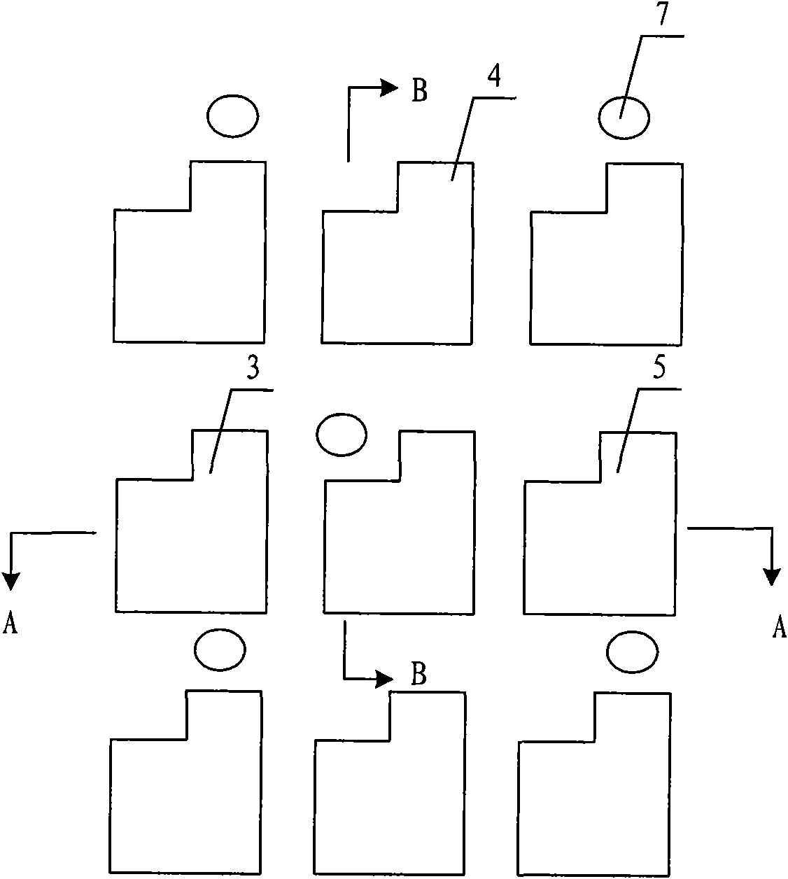
[0037] Figure 4 It is a schematic structural diagram of Embodiment 1 of the liquid crystal display device of the present invention, as Figure 4 As shown, the liquid crystal display device includes an array substrate 9 , a color filter substrate, and a liquid crystal layer 10 disposed between the array substrate 9 and the color filter substrate. Wherein, the color filter substrate includes a substrate 1 , a color pixel pattern and a black matrix pattern 2 . The color pixel pattern is arranged on the substrate 1 in matrix form, for example, Figure 4 The medium-color pixel patterns may include red pixel patterns 3 , green pixel patterns 4 and blue pixel patterns 5 . The black matrix pattern 2 may include a horizontal structure and a vertical structure. The black matrix pattern 2 is supported between the array substrate 9 and the color filter substrate and partly in contact with the array substrate 9, for shading and maintaining the distance between the array substrate 9 and ...


PUM


Abstract

The invention discloses a liquid crystal display device and a manufacture method of a color film substrate thereof. The liquid crystal display device comprises an array substrate, a color film substrate and a liquid crystal layer arranged between the array substrate and the color film substrate, wherein the color film substrate comprises a substrate, a color pixel graph and a black matrix graph, wherein the color pixel graph is arranged on the substrate in a matrix mode; the black matrix graph comprises a transverse structure and a vertical structure, is supported between the array substrate and the color film substrate, is in partial contact with the array substrate and is used for shading light and keeping the liquid crystal box thickness between the array substrate and the color film substrate. Compared with columnar spacers in the prior art, the black matrix graph of the color film substrate increases the supporting area so that the stability of the liquid crystal box thickness is increased to a large degree, and thereby, TOUCH MURA badness is effectively improved, and light leak badness and contrast reduction phenomena brought by observing from different viewing angles are effectively prevented.

Description

technical field [0001] The invention relates to the field of liquid crystal display manufacturing, in particular to a liquid crystal display device and a method for manufacturing a color filter substrate. Background technique [0002] With the development of liquid crystal display technology, thin film transistor liquid crystal display devices (TFT LCD) featuring low power consumption, relatively low manufacturing cost and no radiation have become the mainstream of the liquid crystal display market. TFT LCD is formed by injecting liquid crystal material between the array substrate and the color filter substrate after the array substrate and the color filter substrate are boxed together. Usually, TFT LCD uses the optical anisotropy and birefringence of liquid crystal molecules to display images. TFT LCD changes the orientation of liquid crystal molecules by applying a voltage to the electrodes on the two substrates to generate an electric field, thereby controlling the amoun...

Claims


Application Information

Patent Timeline
IPC IPC(8): G02F1/1335G03F7/00G03F1/00
CPCG02F1/13394G03F7/0007G02F1/133512
Inventor 陈维涛赵凯
Owner BEIJING BOE OPTOELECTRONCIS TECH CO LTD
Learn More