Waveguide coupling metal photonic crystal biosensor and detecting method thereof
A technology of metal photonic crystals and biosensors, applied in instruments, measuring devices, scientific instruments, etc., can solve the problems of cumbersome system operation, long test cycle, and high preparation technology requirements
- Summary
- Abstract
- Description
- Claims
- Application Information
AI Technical Summary
Problems solved by technology
Method used
Image
Examples
Embodiment 1
[0097] This embodiment is a front transmissive waveguide coupling one-dimensional metal photonic crystal biosensor and its detection method:
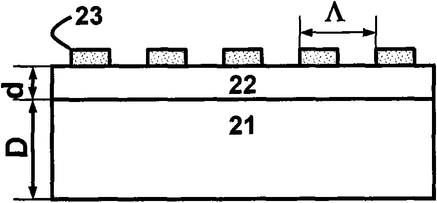
[0098] The substrate 21 used in this embodiment is made of glass with thickness D=1mm, and the waveguide layer 22 is made of indium tin oxide (ITO) thin film glass sheet with thickness d=200nm.
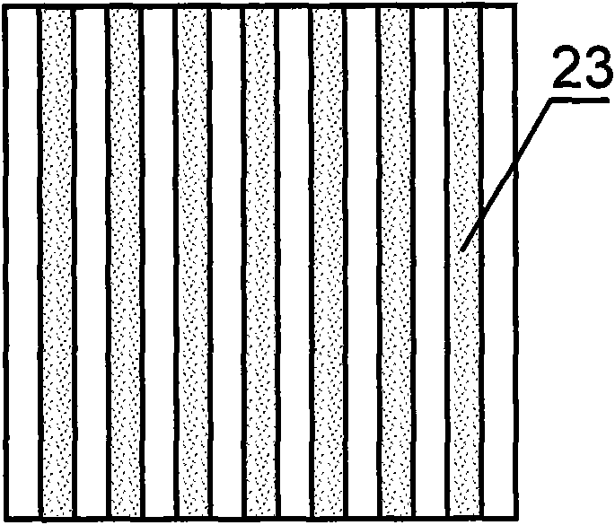
[0099] In this embodiment, a one-dimensional gold photonic crystal with a period of Λ=330nm is prepared on the ITO waveguide layer of a glass substrate by a preparation method of interference lithography combined with a solution method, and a waveguide-coupled one-dimensional gold photonic crystal biosensor is obtained. When using this sensor for detection, the detection method is as follows:
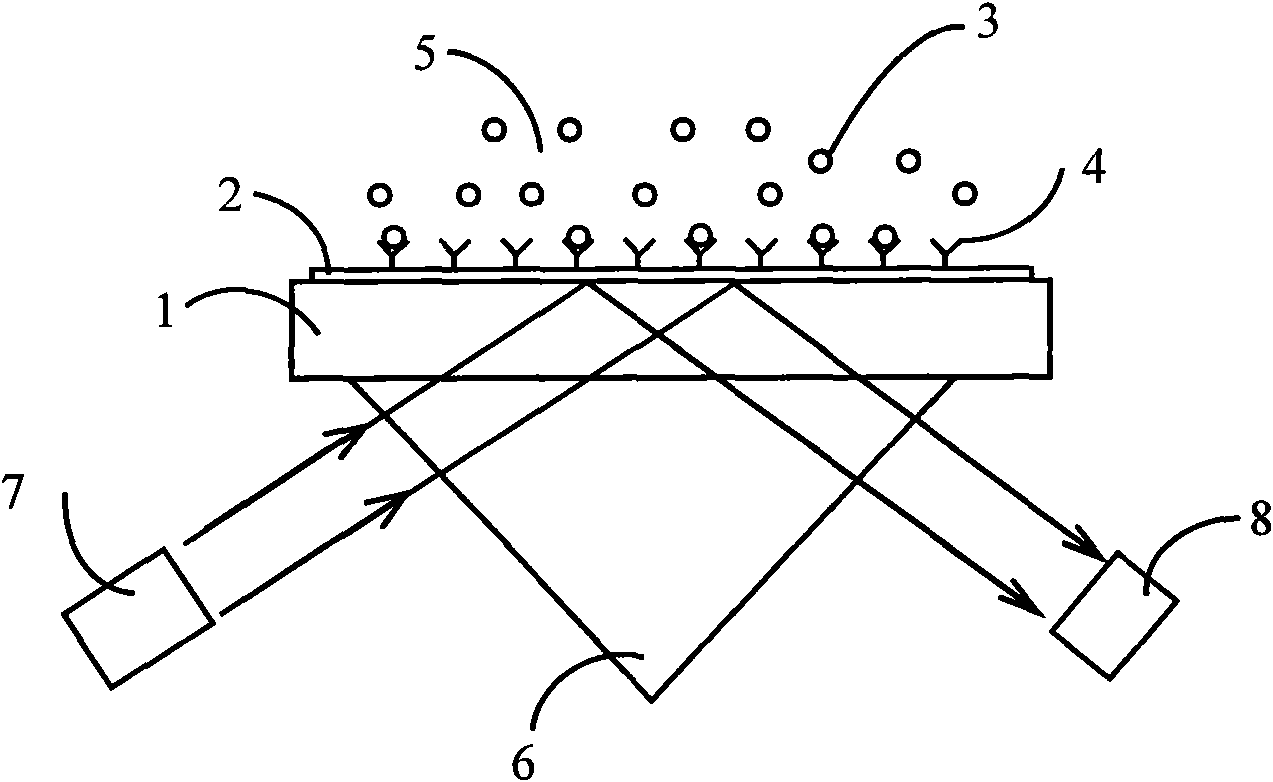
[0100] 1) A receptor (antibody) 4 with a specific recognition function for the ligand (antigen) 3 is immobilized on the surface of the metal photonic crystal 23 in the waveguide-coupled one-dimensional metal photonic crystal biosensor to form the initial...
Embodiment 2
[0106] This embodiment is a back transmission type two-dimensional waveguide coupling metal photonic crystal biosensor and its detection method:
[0107] The substrate used in this embodiment is glass with a thickness of D=1mm, and the waveguide layer is made of ITO glass sheet with a thickness of d=200nm.
[0108] In this example, two-dimensional gold photonic crystals with Λ=350nm period in both directions were prepared on the ITO waveguide layer of the glass substrate by the preparation method of interference lithography combined with the solution method, and a waveguide-coupled two-dimensional gold photonic crystal biosensor was obtained. When using this sensor for detection, the detection method is as follows:
[0109] 1) Immobilize the receptor (antibody) 4 that has a specific recognition function for the ligand (antigen) 3 on the surface of the metal photonic crystal in the two-dimensional waveguide-coupled metal photonic crystal biosensor to form the initial diaphragm ...
Embodiment 3
[0115] This embodiment is a front reflective waveguide coupling one-dimensional metal photonic crystal biosensor and its detection method:
[0116] The substrate used in this embodiment is glass with a thickness of D = 1 mm, and the waveguide layer is an ITO glass sheet with a thickness of d = 210 nm.
[0117] In this embodiment, a one-dimensional gold photonic crystal with a period of Λ=400nm is prepared on an ITO waveguide of a glass substrate by a preparation method of interference lithography combined with a solution method, and a waveguide-coupled one-dimensional gold photonic crystal biosensor is obtained;
[0118] 1) Immobilize the antibody with specific recognition function on the antigen on the surface of the metal photonic crystal in the waveguide-coupled one-dimensional metal photonic crystal biosensor to form the initial diaphragm of the sensor, and contact the blank sample solution with the surface of the metal photonic crystal 23 ;
[0119] 2) The spectral test ...
PUM
| Property | Measurement | Unit |
|---|---|---|
| thickness | aaaaa | aaaaa |
| thickness | aaaaa | aaaaa |
| thickness | aaaaa | aaaaa |
Abstract
Description
Claims
Application Information
 - Generate Ideas
- Intellectual Property
- Life Sciences
- Materials
- Tech Scout
- Unparalleled Data Quality
- Higher Quality Content
- 60% Fewer Hallucinations
Browse by: Latest US Patents, China's latest patents, Technical Efficacy Thesaurus, Application Domain, Technology Topic, Popular Technical Reports.
© 2025 PatSnap. All rights reserved.Legal|Privacy policy|Modern Slavery Act Transparency Statement|Sitemap|About US| Contact US: help@patsnap.com


