
Method for manufacturing semiconductor element with concave-convex base plate

A manufacturing method and semiconductor technology, applied in the direction of semiconductor devices, electrical components, circuits, etc., can solve problems such as complex process procedures

Inactive Publication Date: 2010-08-11
UBILUX OPTOELECTRONICS CORP
View PDF2 Cites 1 Cited by
  • Summary
  • Abstract
  • Description
  • Claims
  • Application Information

AI Technical Summary

Problems solved by technology

[0009] In view of this, the object of the present invention is to provide a method for manufacturing a semiconductor element with a concave-convex substrate, so as to improve the brightness of light-emitting diodes and solve the problem of complicated manufacturing procedures

Method used


Image

  • Method for manufacturing semiconductor element with concave-convex base plate
  • Method for manufacturing semiconductor element with concave-convex base plate
  • Method for manufacturing semiconductor element with concave-convex base plate

Examples


Embodiment Construction

[0025] The method for manufacturing a semiconductor device with a concave-convex substrate according to an embodiment of the present invention will be described below with reference to related drawings. For ease of understanding, the same components in the following embodiments are described with the same symbols.

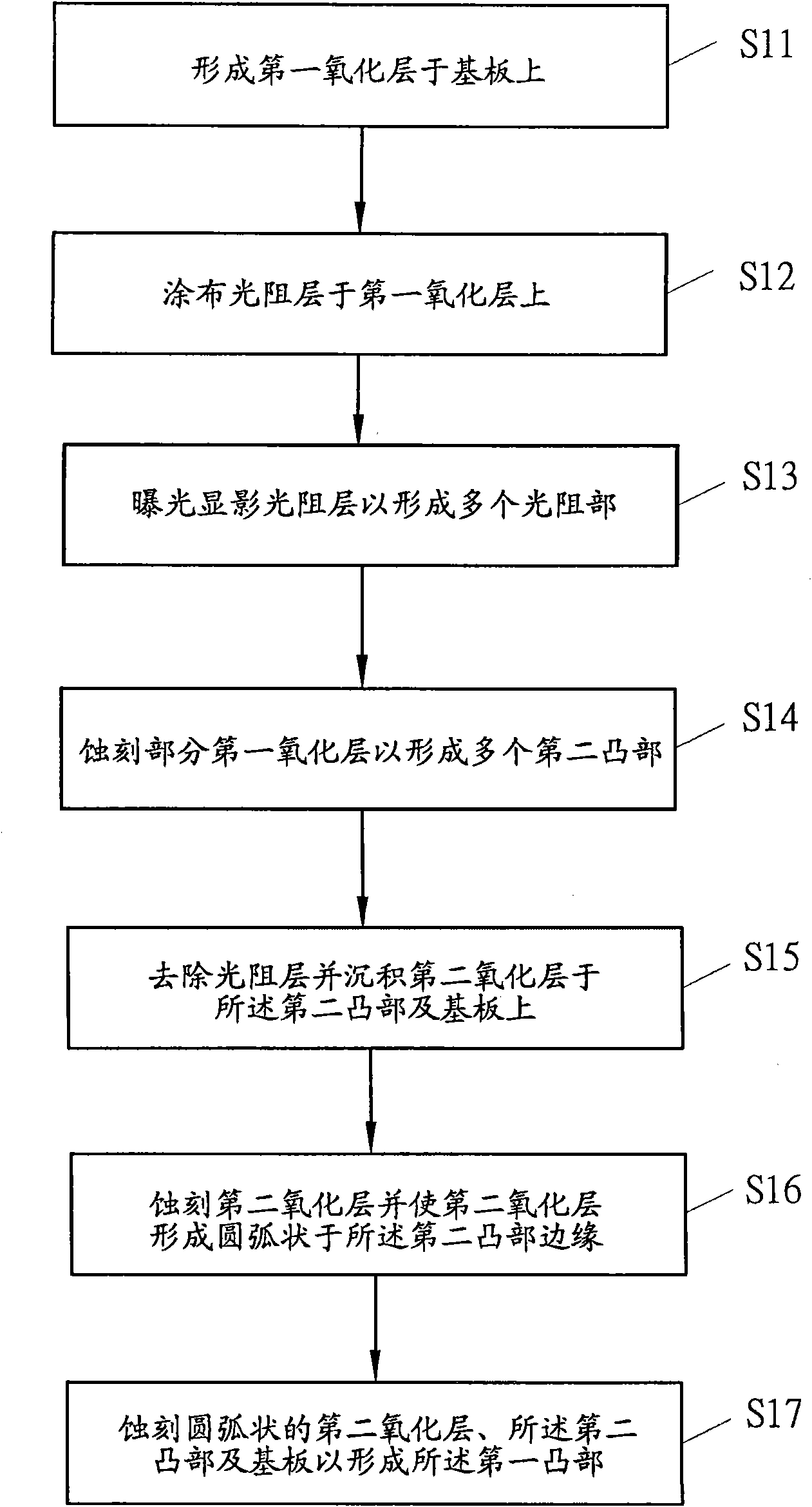
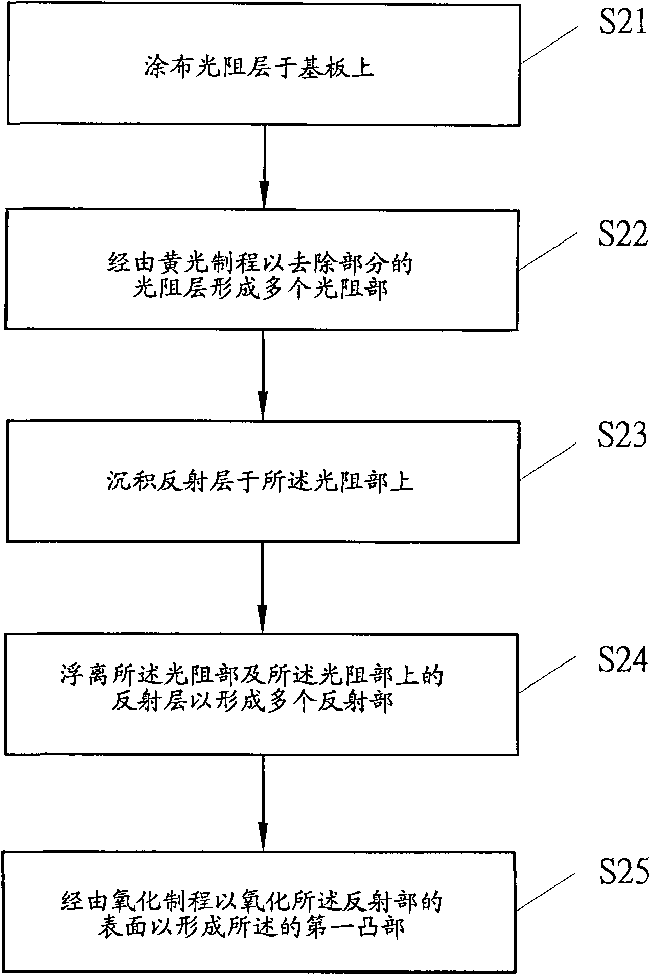
[0026] Figure 1A It is a flow chart of the first embodiment of the method for manufacturing a semiconductor element with a concave-convex substrate of the present invention. The semiconductor element has a substrate and a plurality of semiconductor layers, and the substrate includes a plurality of first protrusions, such as Figure 1A As shown, the manufacturing method includes: in step S11, forming a first oxide layer on the substrate; in step S12, coating a photoresist layer on the first oxide layer; in step S13, exposing and developing the photoresist layer to form multiple a photoresist; in step S14, etching the first oxide layer not covered by the photoresist ...


PUM


Abstract

The invention discloses a method for manufacturing a semiconductor element with a concave-convex base plate. The semiconductor element is provided with a base plate and a plurality of semiconductor layers, wherein the base plate comprises a plurality of first convex parts. The manufacture method comprises the following steps of: forming first oxidation layers on the base plate; coating a plurality of photoresistance parts on the first oxidation layers; etching part of the first oxidation layers to form a plurality of second convex parts; removing photoresistance layers and depositing second oxidation layers on the second convex parts and the base plate; etching the second oxidation layers and enabling the second oxidation layers to form cambered shapes on the edges of the second convex parts; and etching the cambered second oxidation layers, the second convex parts and the base plate to form the first convex parts.

Description

technical field [0001] The invention relates to a method for manufacturing a semiconductor element, in particular to a method for manufacturing a semiconductor element with a concave-convex substrate. Background technique [0002] At present, light-emitting diodes have gradually replaced existing light sources due to their advantages of power saving and high durability. Light-emitting diodes (LEDs) are widely used, including optical display devices, traffic signs, data storage devices, communication devices, and lighting devices. High-brightness LEDs can bring better usage effects, so how to increase the brightness of LEDs has become the biggest issue now. [0003] The basic structure of a light-emitting diode is to grow an n-type semiconductor layer, a light-emitting layer, a p-type semiconductor layer, and electrodes on a substrate. The light-emitting layer uses the combination of electrons and holes to generate visible light and emit it to the outside. [0004] In the p...

Claims


Application Information

Patent Timeline
IPC IPC(8): H01L33/00
Inventor 吴哲雄林志胜
Owner UBILUX OPTOELECTRONICS CORP
Learn More