Controlled dual-output bootstrap circuit

A bootstrap circuit and dual output technology, which is applied in the direction of logic circuit connection/interface layout, logic circuit coupling/interface using field effect transistors, etc., can solve problems such as the drop in the output voltage of the bootstrap circuit and the decrease in the linearity of the output signal. Achieve the effect of enhancing flexibility and improving flexibility

Inactive Publication Date: 2011-11-16
NO 24 RES INST OF CETC
View PDF1 Cites 0 Cited by
  • Summary
  • Abstract
  • Description
  • Claims
  • Application Information

AI Technical Summary

Problems solved by technology

However, the shortcoming of this circuit is: when the timing signal φ is high level, M 7 The gate voltage is V DD ,M 7 work in saturation region, through M 7 to M 7 source and M 10 The parasitic capacitance at the drain node is charged, and the output voltage of the bootstrap circuit will decrease linearly and slowly with time, causing the sampling switch M 11 source voltage D OUT slow down over time
For example, when a DC voltage with an input amplitude of 1V is input, within 20ns, the amplitude of the output voltage will drop by more than 1mV. This is a sample-and-hold circuit applied to a 14 or 16-bit high-speed, high-precision pipeline A / D converter. This phenomenon will cause the linearity of the output signal of the sample and hold circuit to decrease by 10-20dB

Method used


Image

  • Controlled dual-output bootstrap circuit
  • Controlled dual-output bootstrap circuit
  • Controlled dual-output bootstrap circuit

Examples


Embodiment Construction

[0024] The specific implementation manners of the present invention are not limited to the following description, and are now further described in conjunction with the accompanying drawings.

[0025] The circuit diagram of the controllable dual-output bootstrap circuit embodied in the present invention is as figure 2 shown. It consists of a timing control circuit unit, a basic bootstrap circuit unit and a bootstrap output voltage control unit. The specific structure, connection relationship and function relationship are the same as the content of the invention in this specification, and will not be repeated here.

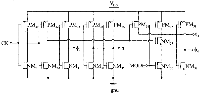
[0026] The circuit diagram of the sequential control circuit unit implemented by the circuit of the present invention is as follows: image 3 shown. Input CMOS level clock signals CK and PM 31 and NM 31 The gate connection of CK through PM 31 and NM 31 Composed of inverters, PM 32 and NM 32 Composed of inverters, PM 33 and NM 33 Output φ after the compose...


PUM


Abstract

The invention discloses a controlled dual-output bootstrap circuit, which comprises a sequential control circuit unit, a basic bootstrap circuit unit and a bootstrap output voltage control unit. The controlled dual-output bootstrap circuit solves the problem that the bootstrap output voltage in the conventional bootstrap circuit descends slowly with time, and the linearity of the bootstrap outputvoltage is improved by 20 dB; on the basis of a basic bootstrap circuit, the controlled dual output of the bootstrap output voltage is realized effectively by adding NMOS pipes NM7, NM8 and NM 9 and PMOS pipes PM5, PM6, PM7 and PM8. The controlled dual-output bootstrap circuit can be widely applied to variable-gain sample-and-hold circuits in high-speed and high-precision analog-digital converters.

Description

technical field [0001] The invention relates to a bootstrap circuit, in particular to a controllable dual-output bootstrap circuit. Its direct application field is the variable gain sampling and holding circuit in high-speed and high-precision analog-to-digital converters. Background technique [0002] Bootstrap circuits are widely used in high-speed and high-precision analog-to-digital converters in analog integrated circuits, mainly in the on-chip sample-and-hold circuits of integrated analog-to-digital converters, to improve the linearity of sampled signals. [0003] A typical bootstrap circuit (US patent, patent number: US 7397284B1, patent name: Bootstrapped circuit) such as figure 1 shown. When the timing signal φ in this circuit is at zero level, the capacitor C 3 The charge stored on the C 3 ×V DD ; When φ is high level, due to the output node (M 9 Gate node) is a high-impedance node without a DC path. According to the principle of charge conservation, M 11 Th...

Claims


Application Information

Patent Timeline
Patent Type & Authority Patents(China)
IPC IPC(8): H03K19/0185
Inventor 刘涛王育新李儒章李婷王妍
Owner NO 24 RES INST OF CETC
Why Eureka
Try Eureka