
Ceramic electronic component

An electronic component and ceramic technology, applied in the field of ceramic electronic components, can solve the problems of difficulty in achieving high capacity and large capacity, difficulty in meeting product size specifications, and large-scale product size.

Active Publication Date: 2010-07-21
TDK CORPARATION
View PDF2 Cites 15 Cited by
  • Summary
  • Abstract
  • Description
  • Claims
  • Application Information

AI Technical Summary

Problems solved by technology

However, in such a method, since the terminal electrode becomes thicker as a whole, the product size is enlarged, and it is difficult to meet the product size specification.
For example, in the case of chip capacitors, if the thickness of the terminal electrodes is increased, it is necessary to reduce the shape and size of the ceramic body in order to meet the product size specifications, and it is difficult to achieve high capacity and large capacity.

Method used


Image

  • Ceramic electronic component
  • Ceramic electronic component
  • Ceramic electronic component

Examples


Embodiment 1

[0066]

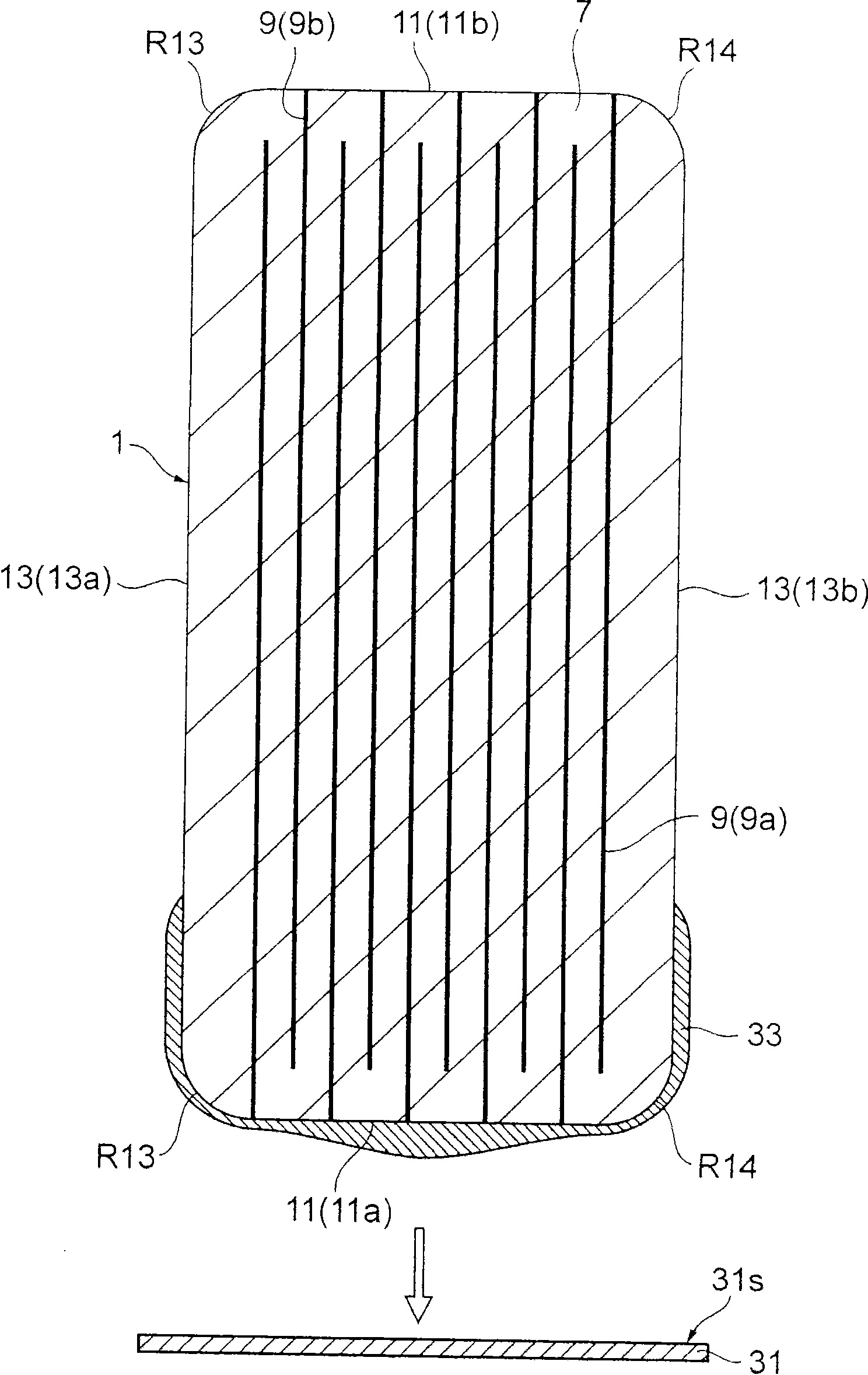
[0067] Mix commercially available BaTiO 3 Powder, binder, organic solvent and plasticizer to prepare ceramic slurry. After coating this ceramic slurry on a PET film using a doctor blade method or the like, it is dried to form a ceramic green sheet.

[0068] An electrode paste mixed with Cu powder or Ni powder with a binder, a solvent, etc. is screen-printed on the formed ceramic green sheet, and dried to form a green sheet with an electrode pattern.

[0069] By repeating the same method, a plurality of green sheets with electrode patterns were formed and laminated to produce a laminated body. Next, the laminated body of the electrode patterned green sheets is cut perpendicular to the lamination direction to form a cuboid-shaped laminated chip, heat-treated, and debonded. The heat treatment is performed at 180 to 400° C. for 0.5 hours or more. The stacked chips obtained by heat treatment are fired at 800-1400°C for 0.5-8.0 hours, and then barrel-polished to chamfe...


PUM


Abstract

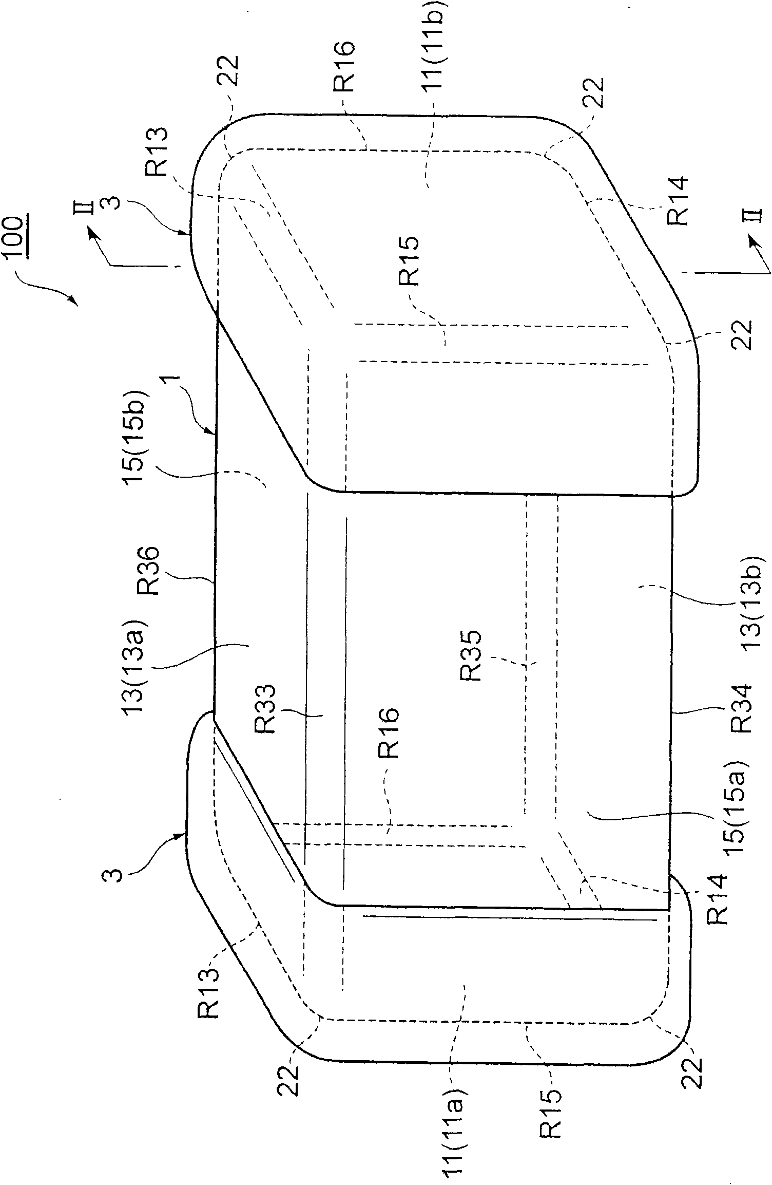
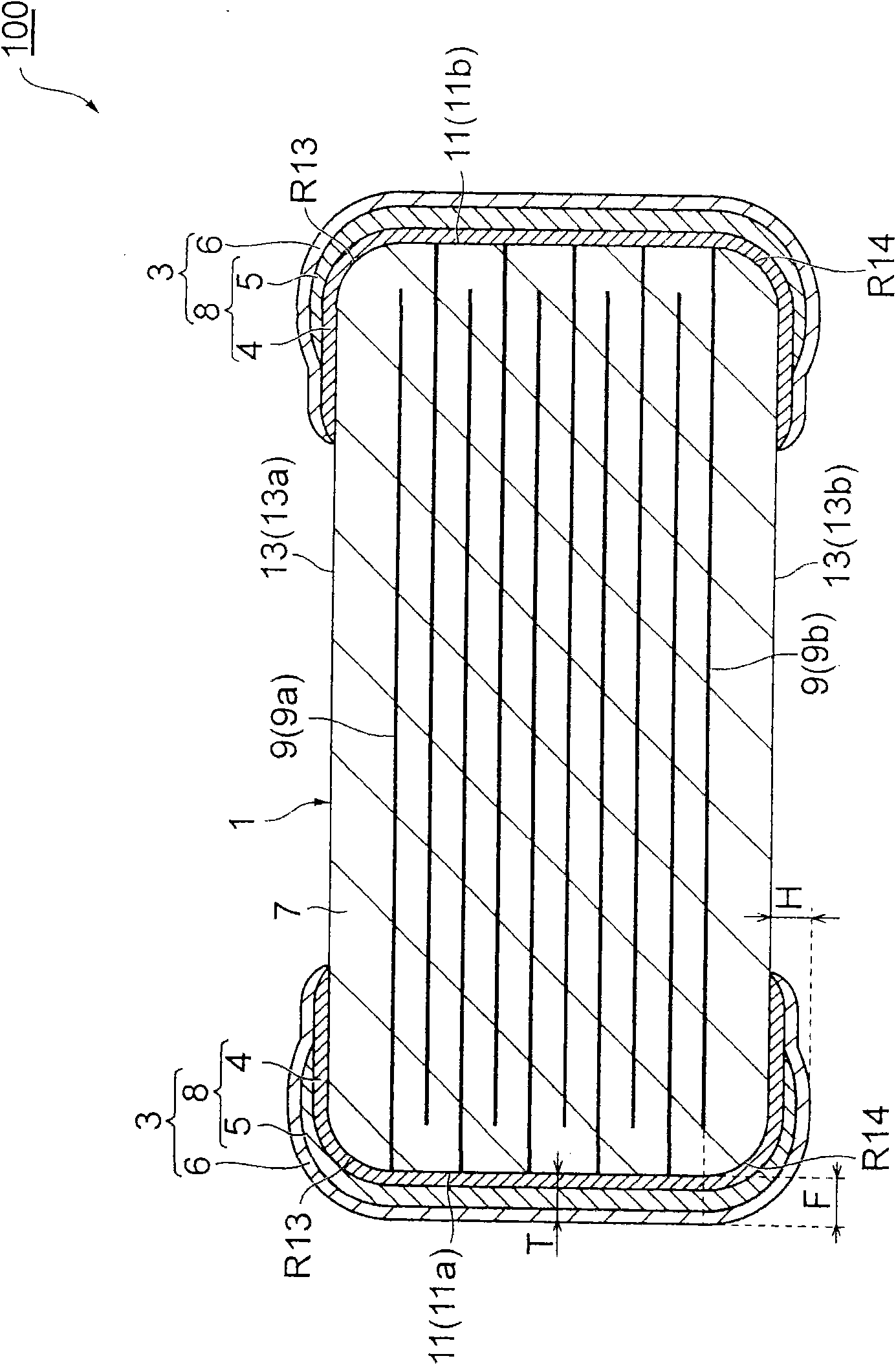
A ceramic electronic part 100 having a chip element 1 having internal electrodes embedded therein, and terminal electrodes 3 that cover the end faces 11 of the chip element 1 having an exposed internal electrode and parts of the side faces 13,15 orthogonal to the end faces 11, and that are electrically connected to the internal electrodes, wherein the terminal electrodes 3 include a first electrode layer and a second electrode layer with a lower glass component content than the first electrode layer, in that order from the chip element 1 side, the second electrode layer being formed covering part of the first electrode layer on the side faces 13,15.

Description

technical field [0001] This invention relates to ceramic electronic components. Background technique [0002] Ceramic electronic components such as laminated ceramic capacitors having a ceramic body and terminal electrodes on end faces thereof are used in various electronic devices and the like. Recently, the miniaturization and high performance of electronic devices are progressing, and along with this, the demand for miniaturization and high capacity of ceramic electronic components is also increasing. [0003] As a technology related to ceramic electronic components, in order to improve the solderability during mounting and the bondability between the ceramic body and the terminal electrodes, it has been proposed to laminate the terminal electrodes of ceramic electronic components with a plurality of electrode layers with different compositions. Structure (for example, refer to JP-A-7-86080 and JP-A-2003-243245). On the outermost layer of the terminal electrodes of this...

Claims


Application Information

Patent Timeline
Patent Type & Authority Applications(China)
IPC IPC(8): H01G4/30H01G4/228
CPCH01G4/2325H01G4/232H01G4/30
Inventor 柳田美幸佐佐木健人栗本哲今野正彦森田友纪阿部寿之
Owner TDK CORPARATION
Learn More