


Quick Research
Generate reliable direction feasibility study reports for your R&D in just a few steps.

Technical Q&A
Discover and master advanced knowledge NOW. Basics, ideas, possibilities, all at once.

Find Solutions
As an expert in R&D theories, this can generate solutions to your technical problems instantly.

Evaluate Feasibility
Analyze your overall solution with one click, know your potential R&D risks in advance.

Monitor Landscape
Get weekly tech updates, stay abreast of the latest tech innovations and key insights.
Phase-change material for compositing VO2 nanometer flower structure on silicon wafer and preparation method thereof
A phase change material, VO2 technology, applied in the fields of nanostructure manufacturing, nanotechnology, nanotechnology, etc., can solve the problems of high cost and harsh conditions, and achieve the effect of low cost, high repeatability and simple growth conditions
- Summary
- Abstract
- Description
- Claims
- Application Information
AI Technical Summary
Problems solved by technology
Method used
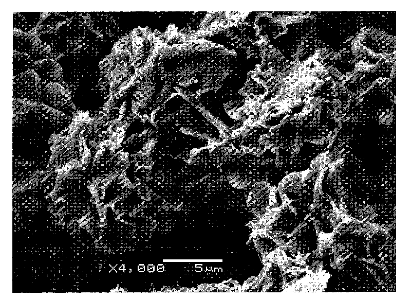
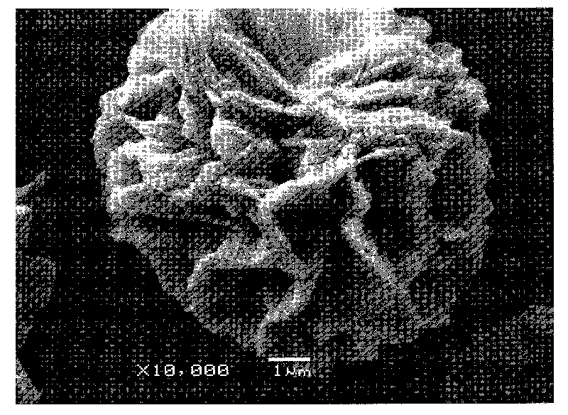
Image


Examples
Embodiment 1
[0020] a. Configure the reaction solution
[0021] 0.75g oxalic acid (C 2 h 2 o 4 ) powder was dissolved in 40ml water, stirred with a magnetic stirrer, after the powder was all dissolved, 0.25g vanadium pentoxide (V 2 o 5 ) powder, continue stirring to form an orange solution;
[0022] b. Growth of VO on silicon wafer 2 nanoflower structure
[0023] First put the cleaned silicon (100) sheet into the autoclave, then pour the above solution into a 50ml autoclave, seal the autoclave, put it into a blast drying oven, and keep the reaction at 160°C for 24 hours , after natural cooling, the composite VO on the silicon wafer was prepared 2 Nanoflower-structured phase change materials.
Embodiment 2
[0025] a. Configure the reaction solution
[0026] 0.85g oxalic acid (C 2 h 2 o 4 ) powder was dissolved in 40ml water, stirred with a magnetic stirrer, after the powder was all dissolved, 0.35g vanadium pentoxide (V 2 o 5 ) powder, continue stirring to form an orange solution;
[0027] b. Growth of VO on silicon wafer 2 nanoflower structure
[0028] First put the cleaned silicon (111) sheet into an autoclave, then pour the above solution into a 50ml autoclave, seal the autoclave, put it into a blast drying oven, and keep the reaction at 150°C for 36 hours , after natural cooling, the composite VO on the silicon wafer was prepared 2 Nanoflower-structured phase change materials.
PUM
| Property | Measurement | Unit |
|---|---|---|
| diameter | aaaaa | aaaaa |
| diameter | aaaaa | aaaaa |
Abstract
Description
Claims
Application Information
 - R&D Engineer
- R&D Manager
- IP Professional
- Industry Leading Data Capabilities
- Powerful AI technology
- Patent DNA Extraction
Browse by: Latest US Patents, China's latest patents, Technical Efficacy Thesaurus, Application Domain, Technology Topic, Popular Technical Reports.
© 2024 PatSnap. All rights reserved.Legal|Privacy policy|Modern Slavery Act Transparency Statement|Sitemap|About US| Contact US: help@patsnap.com