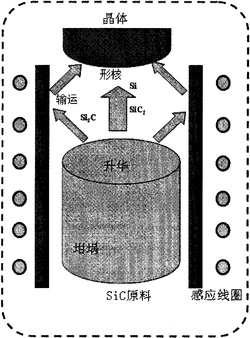
Method for growing high-quality conductive silicon carbide crystal
A silicon carbide and conductive type technology, which is applied in the field of growing high-quality conductive silicon carbide crystals, can solve the problems of limited output, high price, restricting the development of high-performance silicon carbide-based devices, etc., to increase output, reduce defects, and reduce costs. Effect
- Summary
- Abstract
- Description
- Claims
- Application Information
AI Technical Summary
Problems solved by technology
Method used
Image
Examples
Embodiment 1
[0041] Put the crucible filled with silicon carbide raw material and bonded seed crystal into the crystal growth furnace. After heating the crystal growth furnace to 300°C, vacuum the crystal growth system to 10 -3 Pa level, and then filled with a certain amount of argon, repeat this step 3 times to wash the system. After scrubbing, start crystal growth: increase the temperature of the system so that the raw material has a high evaporation temperature (2500-2700°C), and the seed crystal has a relatively low temperature (2100-2300°C); control the mixing of nitrogen and argon in the system The gas pressure was 0.01 Pa, and crystal growth was performed. After the growth, the power was turned off, and the product was cooled to room temperature with the furnace. Take out grown crystals, slice, surface process, and characterize. The growth rate of the obtained crystal was 3 mm / h. figure 2Shown the X-ray diffraction spectrum of wafer after processing, three points on wafer (cent...
Embodiment 2
[0043] Put the crucible filled with silicon carbide raw material and bonded seed crystal into the crystal growth furnace. After heating the system to 400 °C, vacuum the crystal growth system to 10 -3 Pa level, and then filled with a certain amount of argon, repeat this step 3 times to wash the system. After the scrubbing, start crystal growth: Raise the temperature of the system so that the raw material has a high evaporation temperature (2300-2500°C), and the seed crystal has a relatively low temperature (1800-2100°C); control the mixed pressure of nitrogen and argon in the system At 200Pa, crystal growth is performed. After the growth, the power was turned off, and the product was cooled to room temperature with the furnace. Take out grown crystals, slice, surface process, and characterize. The growth rate of the resulting crystal was 1.0 mm / h. Figure 4 Shown the X-ray diffraction spectrum of wafer after processing, three points on wafer (central point, central point pr...
PUM
 Abstract
Description
Claims
Application Information
 - R&D
- Intellectual Property
- Life Sciences
- Materials
- Tech Scout
- Unparalleled Data Quality
- Higher Quality Content
- 60% Fewer Hallucinations
Browse by: Latest US Patents, China's latest patents, Technical Efficacy Thesaurus, Application Domain, Technology Topic, Popular Technical Reports.
© 2025 PatSnap. All rights reserved.Legal|Privacy policy|Modern Slavery Act Transparency Statement|Sitemap|About US| Contact US: help@patsnap.com


