
Manufacture method of MEMS packaged glass microcavity with optical window

A technology for encapsulating glass and optical windows, used in optics, manufacturing tools, manufacturing microstructure devices, etc., can solve the problems of surface roughness of glass microcavities, difficult to achieve surface roughness of optical devices, and poor bottom surface roughness of glass microcavities.

Inactive Publication Date: 2010-05-05
JIANGSU XINGSHA GLASS TECH +1
View PDF0 Cites 10 Cited by
  • Summary
  • Abstract
  • Description
  • Claims
  • Application Information

AI Technical Summary

Problems solved by technology

However, since the Si surface is very rough during the etching process, and the glass softens during the thermoforming process, it is in close contact with the etched Si deep cavity, so the surface of the glass microcavity is also very rough, and it is difficult to meet the packaging requirements of optical devices. surface roughness
The other type is to use the method of blowing glass spheres to manufacture glass microcavity arrays. Since the glass surface that is anodically bonded to the Si mold will etch off the Si layer, and the glass surface will be bonded with the Si of the MEMS device. Secondary anodic bonding, so that even though the surface roughness of the glass ball cavity is very good, the bottom surface roughness of the glass microcavity is very poor due to the primary bonding, so it is difficult to perform secondary anodic bonding to package MEMS devices

Method used


Image

  • Manufacture method of MEMS packaged glass microcavity with optical window
  • Manufacture method of MEMS packaged glass microcavity with optical window
  • Manufacture method of MEMS packaged glass microcavity with optical window

Examples


Embodiment 1

[0028] A method for manufacturing a wafer-level glass microcavity, comprising the following steps:

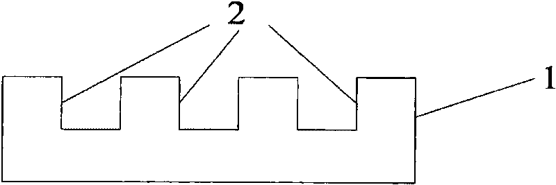
[0029] In the first step, a specific microgroove pattern is formed by etching on a Si wafer (such as a 4-inch wafer) using a Si micromachining process. The micromachining process of the pattern structure on the Si original sheet is a wet etching process or a dry induction process. One of the coupled plasma (ICP) etching process, reactive ion etching or deep reactive ion etching, the pattern can be a square or circular groove array, or a number of different graphics, (actually three-dimensional Look, engraving a specific pattern is to carve a groove on a silicon wafer, which is a pattern in two dimensions), and the aspect ratio of the microgroove can be less than 1:1 or greater than 1:1, for example: 2:1, 3:1, 4 : 1, 7: 1, 10: 1, 15: 1, 20: 1, glass microcavities with large aspect ratio will provide more rheological space for the glass, thus providing more options for the size o...

Embodiment 2

[0035] A method for manufacturing a wafer-level glass microcavity, comprising the following steps:

[0036] The first step is to etch a specific pattern on a 4-inch Si wafer by using deep reactive ion etching (in fact, in three dimensions, it is a groove on the silicon wafer, and in two dimensions, it is a pattern). The pattern is a square groove array , the aspect ratio of the pattern is 20:1, the silicon wafer is polished,

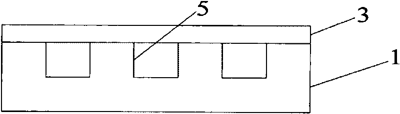
[0037] In the second step, the above-mentioned Si wafer and the (4 inches) Pyrex7740 glass wafer of the same size (a brand of borosilicate glass, produced by Corning-corning in the United States, available in the market, have been polished) in an atmosphere of 1000Pa The bonding is carried out on the EVG-501 anode bonding machine, so that the above-mentioned specific pattern on the Pyrex7740 glass forms a sealed cavity, and the bonding surface is routinely cleaned and polished according to the requirements of anodic bonding before bonding to maintain a h...


PUM


Abstract

The invention discloses a manufacture method of an MEMS packaged glass microcavity with an optical window, which comprises the following steps of: firstly, etching a special microgroove pattern on a silicon wafer by using an Si micromachining process; secondly, bonding the silicon wafer etched with the microgroove and a Pyrex7740 glass wafer under an atmosphere pressure of 100Pa-30kPa to enable the Pyrex7740 glass wafer and the special pattern to form a closed cavity; and thirdly, heating the bonded wafer under high atmospheric pressure, preserving the temperature, enabling softened glass to protrude towards the closed cavity to form a spherical surface by using the difference of pressures inside and outside the cavity so as to form a microcavity structure corresponding to the microcavity pattern structure, cooling, annealing to eliminate the stress under normal pressure, wherein the spherical surface is not in contact with the bottom of the microgroove of the silicon wafer. The method is simple and is low in cost; in addition, an optical channel with a smooth surface is formed, and a smooth bonding surface is provided.

Description

technical field [0001] The invention relates to a MEMS (micro-electro-mechanical system) packaging technology, in particular to a method for manufacturing a MEMS packaging glass microcavity with an optical window. Background technique [0002] In the field of MEMS packaging, since devices generally contain movable parts, it is necessary to use a micron-sized microcavity structure to hermetically package the device during packaging, so that the movable parts have room for movement and provide physical protection for the device. Some such as Devices such as resonators, gyroscopes, and accelerometers also require a vacuum and airtight packaging environment. The cavity made of inorganic material glass can provide a better vacuum and sealing environment, and the anodic bonding process can provide very good air tightness, which is the most commonly used vacuum sealing bonding process. The vacuum packaging of MEMS devices can be achieved by forming a microcavity structure on Pyrex...

Claims


Application Information

Patent Timeline
IPC IPC(8): B81C1/00B81C3/00
Inventor 尚金堂徐超张迪陈波寅柳俊文唐洁影黄庆安
Owner JIANGSU XINGSHA GLASS TECH
Learn More