Method for producing stepped PCB board

A technology of a PCB board and a production method, which is applied in the production field of stepped PCB boards, can solve the problems of difficulty in precise positioning of stepped grooves, difficulty in accurately controlling the size and depth of stepped grooves, and difficulty in ensuring that the walls of the stepped grooves are neat and free of defects, etc. The effect of positioning, controllable cutting depth and less process

Active Publication Date: 2010-04-28
SHANGHAI MEADVILLE ELECTRONICS
View PDF0 Cites 29 Cited by
  • Summary
  • Abstract
  • Description
  • Claims
  • Application Information

AI Technical Summary

Problems solved by technology

However, due to the large error between the mechanical milling core board and the prepreg, the lamination method and other factors, the current method is still difficult to accurately locate the position of the stepped groove, it is difficult to accurately control the size and depth of the stepped groove, and it is difficult to ensure that the walls of the stepped groove are neat no defect issues

Method used


Image

  • Method for producing stepped PCB board
  • Method for producing stepped PCB board
  • Method for producing stepped PCB board

Examples


Embodiment 1

[0026] The production method of ladder PCB board comprises the following steps:

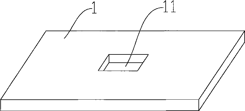
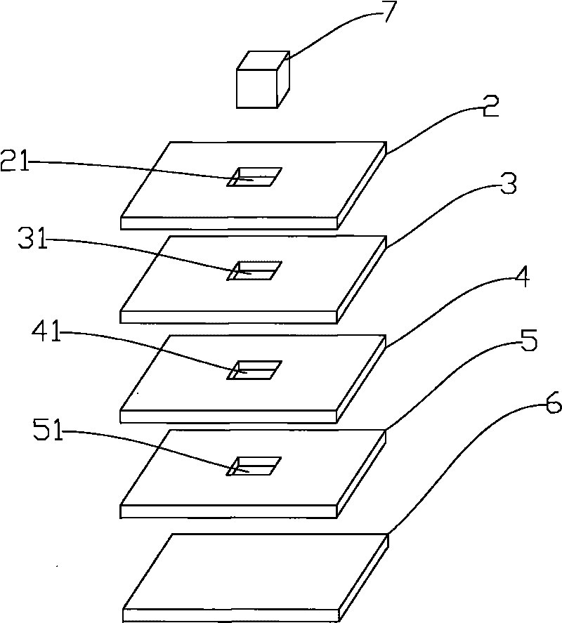
[0027] Such as Figure 4 As shown, a, the inner layer core plate 4 has a window 41;

[0028] b. The first prepreg 3 and the second prepreg 5 are pasted on both surfaces of the inner core board 4 respectively, the first prepreg 3 pre-opens the window 31, the second prepreg 5 pre-opens the window 51, the positions of the window 31, the window 51 and the window 41 Alignment; after this step is completed, the inner core board 4 is sandwiched between the first prepreg 3 and the second prepreg 5;

[0029] c. Put the silica gel sheet 7 into the windows 31, 41, and 51; the thickness of the silica gel sheet 7 is approximately equal to the sum of the thicknesses of the first prepreg 3, the inner core board 4 and the second prepreg 5.

[0030] d, the first outer layer core board 2 is arranged on the surface of the first prepreg 3, and the second outer layer core board 6 is arranged on the surface of the s...

Embodiment 2

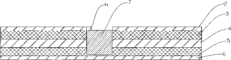
[0036] Such as Figure 6 Shown is the side cross-sectional view before cutting after the components of the PCB board in Example 2 are superimposed. On the basis of Example 1, a third prepreg 8 is attached to the surface of the first outer core board 2, a first copper foil 9 is attached to the surface of the third prepreg 8, and a fourth prepreg is attached to the surface of the second outer core board 6. 10. A second copper foil 11 is attached on the surface of the fourth prepreg 10 . All the other steps are the same as in Example 1.

Embodiment 3

[0038] On the basis of Example 2, both the first copper foil and the second copper foil are replaced by core boards. Other steps and structure are identical with embodiment 2.


PUM


Abstract

The invention discloses a method for producing a stepped PCB board, which is characterized by comprising the following steps: a, windowing an inner core board; b, respectively pasting windowed prepregs on two surfaces of the inner core board, and making windows on the prepregs opposite to the window on the inner core board; c, putting silicon sheets into the windows on the inner core board and the prepregs; d, respectively arranging an outer core board on the surfaces of the two prepregs, and performing lamination; and e, cutting a stepped groove with laser, and taking the silicon sheets and the cut outer core boards out to form the stepped PCB board. In the method, the position of the stepped groove can be precisely positioned, the size and depth of the stepped groove are precisely ensured, and the groove wall of the stepped groove is neat and non-defective; the laminated panel and the silicon sheets after laser cutting can be easily taken out, and do not stick to the groove bottom; in addition, the inner core board and the prepregs are required to be windowed only, and other plates are not required to be windowed, so the working procedures are less. The method is simple, effective and convenient to implement, and is suitable for processing the stepped PCB board.

Description

technical field [0001] The invention relates to a production method of a stepped PCB board. Background technique [0002] Such as figure 1 As shown, it is a multi-layer PCB board 1 with a groove 11 on it. The groove 11 is also called a stepped groove, which is a non-through groove. In the present invention, this kind of PCB board is referred to as a stepped PCB board for short. [0003] The production method of the stepped PCB board in the prior art is to attach prepregs on both surfaces of the inner core board, and then attach copper foil or outer core boards on the surface of the prepreg, and laminate at high temperature. The prepreg is mainly composed of thermoplastic resin, which is solid at room temperature and turns into a semi-fluid liquid at high temperature. When it returns to normal temperature after lamination, the prepreg will bond the multi-layer inner core board, outer core board or copper foil into one. When producing stepped PCB boards, such as figure 2...

Claims


Application Information

Patent Timeline
Patent Type & Authority Applications(China)
IPC IPC(8): H05K3/00H05K3/46
Inventor 屈刚赵国强陈晓峰黄伟曹立志
Owner SHANGHAI MEADVILLE ELECTRONICS
Why Eureka
Try Eureka