
Filling method of deep groove isolation structure of silicon-on-insulator

A silicon-on-insulator and isolation structure technology, which is applied in semiconductor/solid-state device manufacturing, electrical components, circuits, etc., can solve the problems of etching gas concentration distribution edge effect, difficulty in controlling the thickness of amorphous silicon, and difficulty in controlling the thickness of oxide layer, etc. , to achieve the effect of avoiding polysilicon void phenomenon, good compactness and high yield

Inactive Publication Date: 2011-05-11
SUZHOU POWERON IC DESIGN
View PDF0 Cites 0 Cited by
  • Summary
  • Abstract
  • Description
  • Claims
  • Application Information

AI Technical Summary

Problems solved by technology

[0007] Aiming at the traditional filling method of the silicon-on-insulator deep trench isolation structure, it has the following disadvantages: due to the existence of the buried oxide layer in the silicon-on-insulator, the concentration distribution of the etching gas at the bottom of the trench during the etching process has an edge effect, that is, the two sides of the trench The concentration of etching ions on the sidewall is higher than that in the middle area
However, in this method, the thickness of the deposited amorphous silicon is difficult to control, and the thickness of the formed oxide layer is also difficult to control, so there is no flexibility.

Method used


Image

  • Filling method of deep groove isolation structure of silicon-on-insulator
  • Filling method of deep groove isolation structure of silicon-on-insulator
  • Filling method of deep groove isolation structure of silicon-on-insulator

Examples


Embodiment Construction

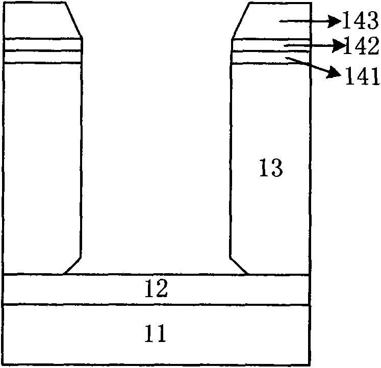
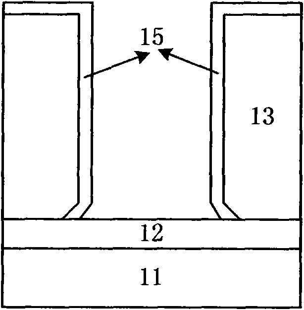
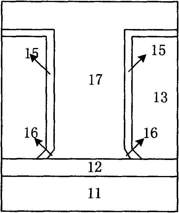
[0030] Please refer to diagram 2-1 , 2-2 , 2-3, 2-4, a silicon-on-insulator deep trench isolation structure adopting a new deep trench filling method, comprising: a semiconductor substrate 1, a buried oxide layer 22 is arranged on the semiconductor substrate 21, and the buried oxide N-type top layer silicon 23 is provided on layer 22, and the morphology of deep grooves is etched on the surface of N-type top layer silicon 23, and the deep groove structure is filled with dielectric, and the surface and side walls of N-type top layer silicon 23 are processed by dry oxygen method. Grow the first layer of oxide layer 24 with a thickness of 100-200 Deposit the first layer of polysilicon 26 on the sidewall of the first layer of oxide layer 24 grown by dry oxygen method, with a thickness of about 13% to 20% of the groove width, and to a greater extent depends on the lateral overetching of the bottom of the deep groove. The size of the polysilicon 26 does not have any doping, and t...


PUM


Abstract

The invention provides a medium filling method of a deep groove isolation structure of silicon-on-insulator, comprising a buried oxide layer which is arranged on the semiconductor substrate; N-shaped top layer silicon is arranged on the buried oxide layer; and the topogram of the deep groove is etched on the surface of the N-shaped top layer silicon. The filling of the deep groove comprises the following steps: growing a first oxide layer through a dry-oxygen method after the top layer silicon is etched; depositing a first layer of polysilicon on the side wall of the first oxide layer grown by the dry-oxygen method; carrying out a wet-oxygen method on the surface of the pure polysilicon to thermally grow a second oxide layer; and finally depositing a second layer of polysilicon on the side wall of the second oxide layer which is thermally grown by the wet-oxygen method. In the filling method of the invention, a first layer of pure polysilicon is deposited on the side wall of the firstoxide layer which is grown by the dry-oxygen method, therefore, on the one hand, the sinking area which is over-etched horizontally at the bottom part of the deep groove is filled, and on the other hand, the growth rate of the isolation oxide layer at the bottom part of the deep groove is improved, thus ensuring the uniformity of the thickness of the isolation oxide layer and improving the deep groove isolation ability of silicon-on-insulator.

Description

technical field [0001] The invention belongs to the field of power semiconductor integrated circuits, in particular to a method for filling a deep groove all-dielectric isolation structure on a silicon-on-insulator (SOI) material. Background technique [0002] In high and low voltage power integrated circuits, one of the biggest challenges is to achieve complete isolation of high and low voltage parts. Because the high-voltage and low-voltage circuits are made on the same substrate, the carriers injected into the substrate by the device will be collected by the adjacent large-area power devices, which may cause false turn-on of the power device, which limits the integration of high-voltage and low-voltage circuits. a major factor. The ideal method for device isolation would be to completely enclose each device in an insulating material. With the increasing maturity of SOI (silicon-on-insulator) bonding technology, the silicon-on-insulator deep trench isolation mechanism ha...

Claims


Application Information

Patent Timeline
Patent Type & Authority Patents(China)
IPC IPC(8): H01L21/762
Inventor 易扬波李海松王钦杨东林
Owner SUZHOU POWERON IC DESIGN
Learn More