Plasma display panel
A display panel and plasma technology, applied in AC plasma display panels, gas discharge electrodes, gas discharge tubes/containers, etc., can solve the problem of increased charge decay rate
- Summary
- Abstract
- Description
- Claims
- Application Information
AI Technical Summary
Problems solved by technology
Method used
Image
Examples
Embodiment approach
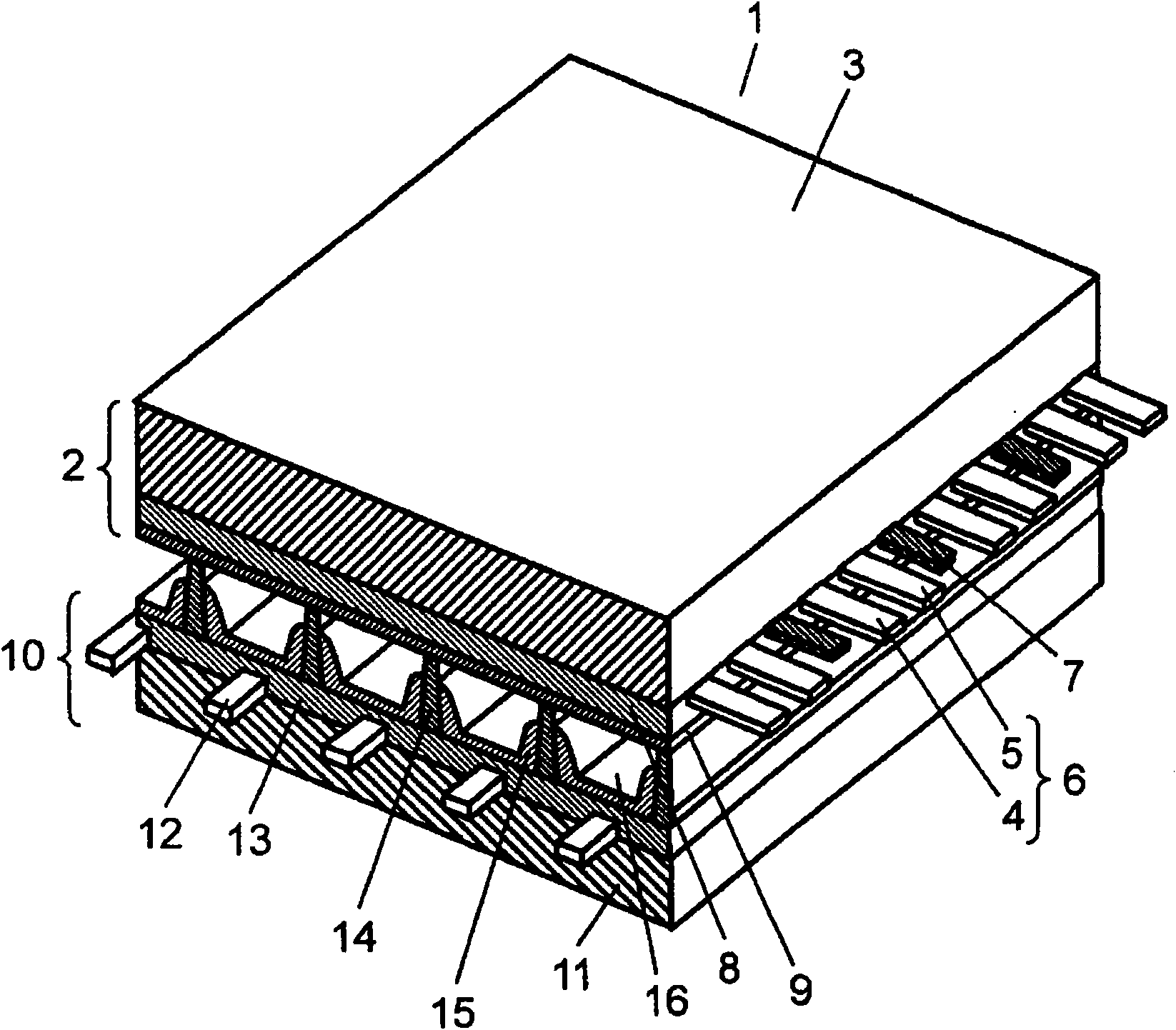
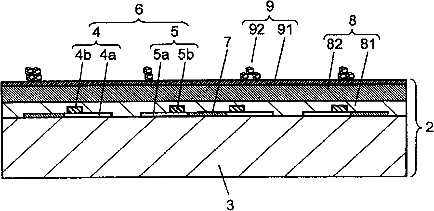
[0049] figure 1 is a side view showing the structure of the PDP according to the embodiment of the present invention. The basic structure of the PDP is the same as that of a common AC surface discharge type PDP. Such as figure 1 As shown, in the PDP 1, the front panel 2 including the front glass substrate 3 and the like and the rear panel 10 including the rear glass substrate 11 and the like are disposed opposite to each other. The outer peripheral portion of the PDP 1 is hermetically sealed with a sealing material including glass frit or the like. Discharge gas such as Ne and Xe is sealed in the discharge space 16 inside the sealed PDP 1 at a pressure of 400 Torr to 600 Torr.
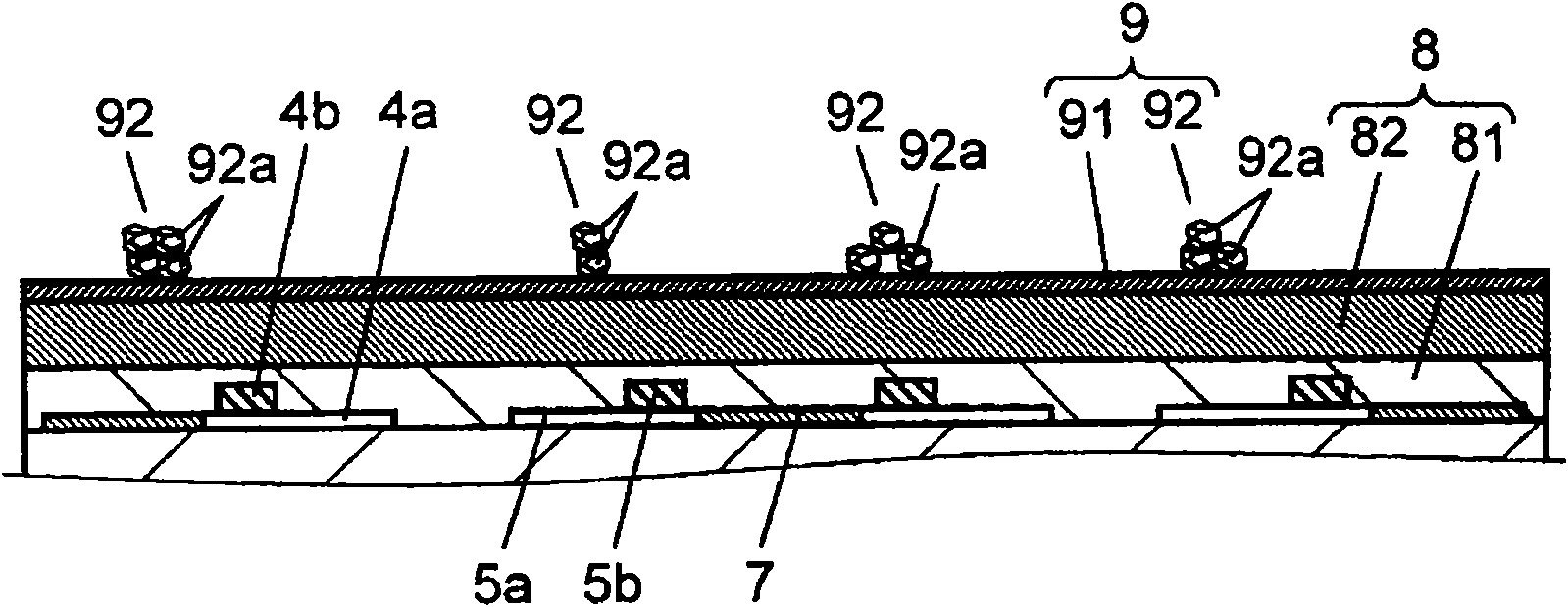
[0050] A pair of strip-shaped display electrodes 6 and black strips (light shielding layers) 7 composed of scan electrodes 4 and sustain electrodes 5 are arranged in parallel on front glass substrate 3 of front panel 2 in multiple rows. A dielectric layer 8 functioning as a capacitor is formed on t...
PUM
| Property | Measurement | Unit |
|---|---|---|
| The average particle size | aaaaa | aaaaa |
| The average particle size | aaaaa | aaaaa |
Abstract
Description
Claims
Application Information
 - R&D
- Intellectual Property
- Life Sciences
- Materials
- Tech Scout
- Unparalleled Data Quality
- Higher Quality Content
- 60% Fewer Hallucinations
Browse by: Latest US Patents, China's latest patents, Technical Efficacy Thesaurus, Application Domain, Technology Topic, Popular Technical Reports.
© 2025 PatSnap. All rights reserved.Legal|Privacy policy|Modern Slavery Act Transparency Statement|Sitemap|About US| Contact US: help@patsnap.com


