Electronic component packing body
一种电子部件、包装体的技术,应用在包装、包装纸、电气元件等方向,能够解决无法进行热密封、阻碍粘接树脂粘着特性、剥离等问题
- Summary
- Abstract
- Description
- Claims
- Application Information
AI Technical Summary
Problems solved by technology
Method used
Image
Examples
Embodiment Construction
[0096] Hereinafter, the present invention will be described in more detail by giving examples, but the present invention is not limited to these examples. In addition, in an Example, unless otherwise indicated, "part" and "%" represent "part by mass" and "% by mass".
[0097] Examples and Comparative Examples
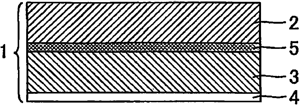
[0098] A base film (substrate layer) with a film thickness of 25 μm was used as the outer layer, and an intermediate layer with a thickness of 15 μm was formed on the base film by extrusion lamination to obtain a film with a total thickness of 40 μm. After activating the surface of the film obtained above by corona treatment, it was coated according to the composition shown in Table 1 and Table 2 (thickness after drying: 1 μm) to form a heat-sealing layer and obtain a film (cover tape) .
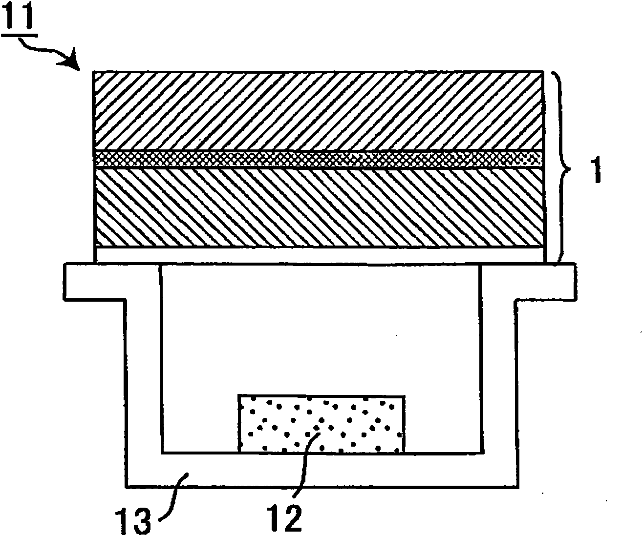
[0099] Mount the electronic components on a 8mm wide polystyrene carrier tape (raw material: polystyrene doped with carbon), cut the cover tape obtained above to a width of 5.5mm, a...
PUM
| Property | Measurement | Unit |
|---|---|---|
| area | aaaaa | aaaaa |
| molecular weight | aaaaa | aaaaa |
| molecular weight | aaaaa | aaaaa |
Abstract
Description
Claims
Application Information
 - R&D
- Intellectual Property
- Life Sciences
- Materials
- Tech Scout
- Unparalleled Data Quality
- Higher Quality Content
- 60% Fewer Hallucinations
Browse by: Latest US Patents, China's latest patents, Technical Efficacy Thesaurus, Application Domain, Technology Topic, Popular Technical Reports.
© 2025 PatSnap. All rights reserved.Legal|Privacy policy|Modern Slavery Act Transparency Statement|Sitemap|About US| Contact US: help@patsnap.com


