


Quick Research
Generate reliable direction feasibility study reports for your R&D in just a few steps.

Technical Q&A
Discover and master advanced knowledge NOW. Basics, ideas, possibilities, all at once.

Find Solutions
As an expert in R&D theories, this can generate solutions to your technical problems instantly.

Evaluate Feasibility
Analyze your overall solution with one click, know your potential R&D risks in advance.

Monitor Landscape
Get weekly tech updates, stay abreast of the latest tech innovations and key insights.
LED device and packaging method thereof
A technology for LED devices and packaging methods, applied in semiconductor devices, electrical components, circuits, etc., can solve the problems that high-power products cannot pass the reflow soldering process, high-power products are seriously damaged, time-consuming and labor-intensive, etc., to avoid light loss, improve Product yield and wide applicability
- Summary
- Abstract
- Description
- Claims
- Application Information
AI Technical Summary
Problems solved by technology
Method used
Image

Examples
Embodiment Construction
[0019] The present invention will be further described below with reference to the accompanying drawings and embodiments.
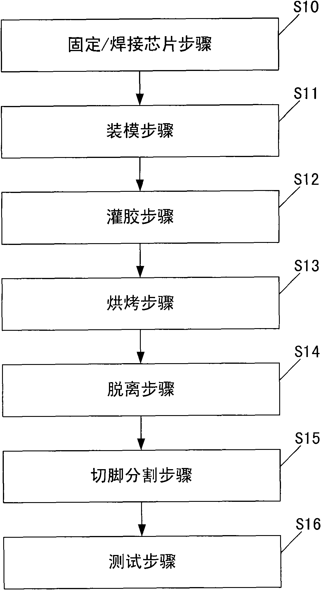
[0020] figure 1 The flow of a preferred embodiment of the packaging method of the LED device of the present invention is shown. See figure 1 , the following is a detailed description of each step in the method.
[0021] Step S10: Fixing / Soldering Step: Fixing the chip and soldering the chip to form a light-emitting unit.
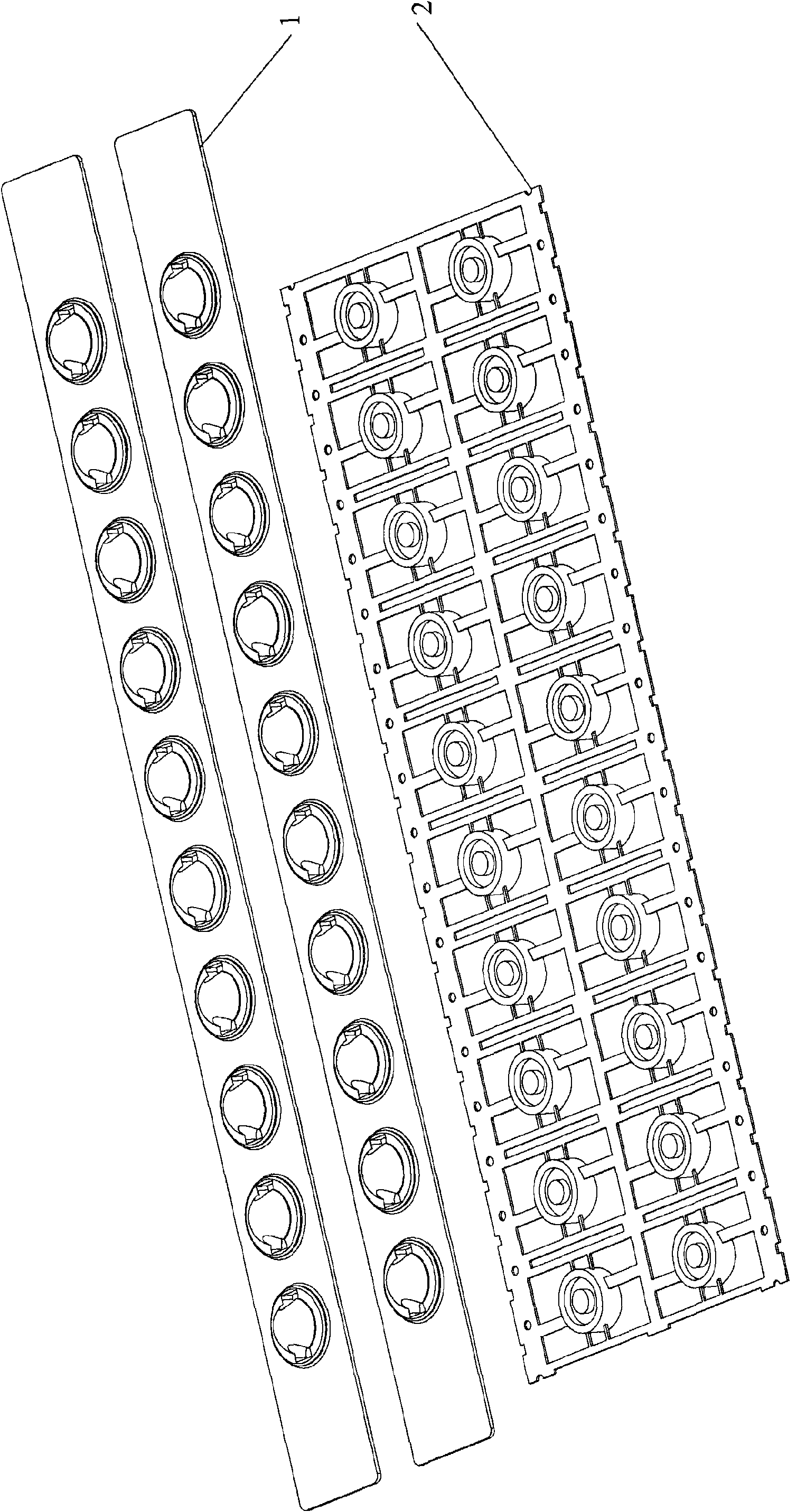
[0022] Step S11: Molding step: see also figure 2 , Fix the bracket 2 with a clamp, place the mold bar 1 on the bracket 2, make the bracket 2 integrally embedded in the mold bar 1, and then fix the mold bar 1 with a clamp to make it completely closed.
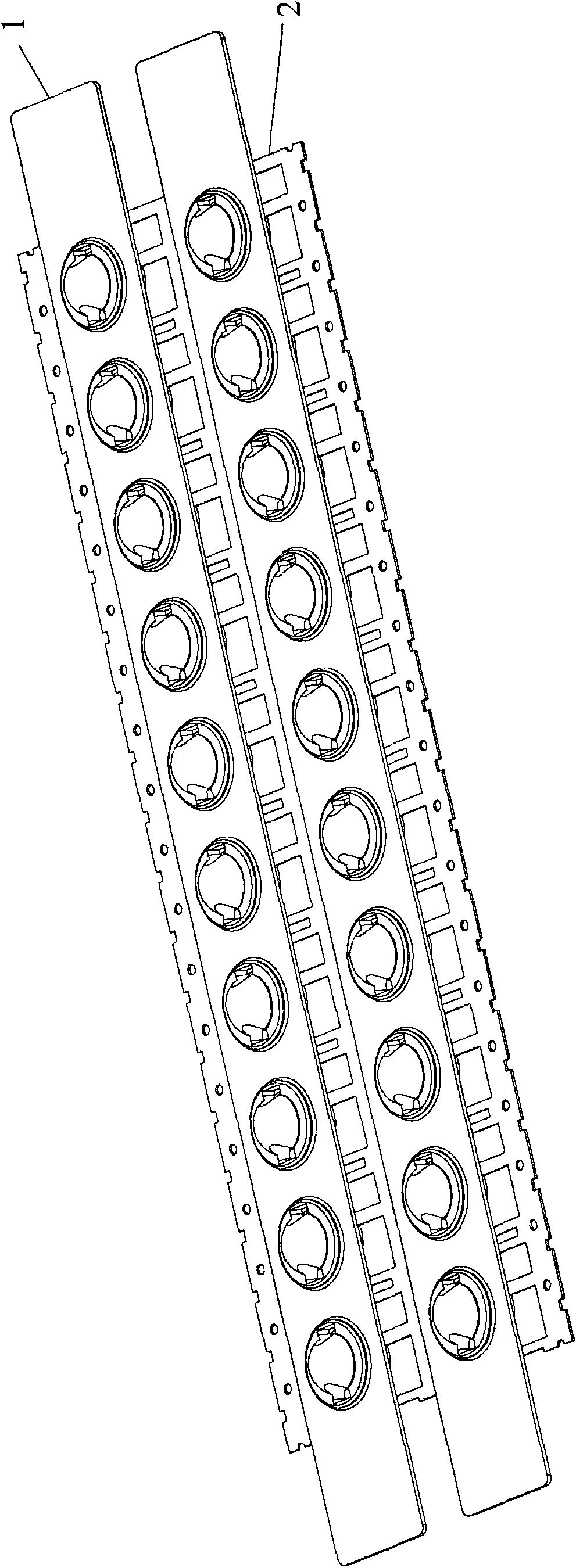
[0023] Step S12: Glue filling step: see also image 3 , use a syringe to inject the silicone from the injection port A until the silicone overflows from the injection port B, control the pressure and time, and press out all the air in the mold bar 1. Different perfusion angles can ...
PUM
 Abstract
Description
Claims
Application Information
 - R&D Engineer
- R&D Manager
- IP Professional
- Industry Leading Data Capabilities
- Powerful AI technology
- Patent DNA Extraction
Browse by: Latest US Patents, China's latest patents, Technical Efficacy Thesaurus, Application Domain, Technology Topic, Popular Technical Reports.
© 2024 PatSnap. All rights reserved.Legal|Privacy policy|Modern Slavery Act Transparency Statement|Sitemap|About US| Contact US: help@patsnap.com