Vertical iii-nitride light emitting diodes on patterned substrates with embedded bottom electrodes

A technology of light-emitting diodes and nucleation layers, applied in electrical components, circuits, semiconductor devices, etc., can solve problems such as complex and expensive methods, increased cost of insulating substrates, and affecting LED performance

Inactive Publication Date: 2010-01-27
TAIWAN SEMICON MFG CO LTD
View PDF0 Cites 4 Cited by
  • Summary
  • Abstract
  • Description
  • Claims
  • Application Information

AI Technical Summary

Problems solved by technology

This method requires chip-bonding LED procedures and removal of the insulating substrate. However, if the junction between the conductor layer and the LED chip is not uniform, it will also affect the performance of the LED.
Furthermore, the removal of the insulating substrate will increase the cost, so the traditional method is complex and expensive

Method used


Image

  • Vertical iii-nitride light emitting diodes on patterned substrates with embedded bottom electrodes
  • Vertical iii-nitride light emitting diodes on patterned substrates with embedded bottom electrodes
  • Vertical iii-nitride light emitting diodes on patterned substrates with embedded bottom electrodes

Examples


no. 1 example

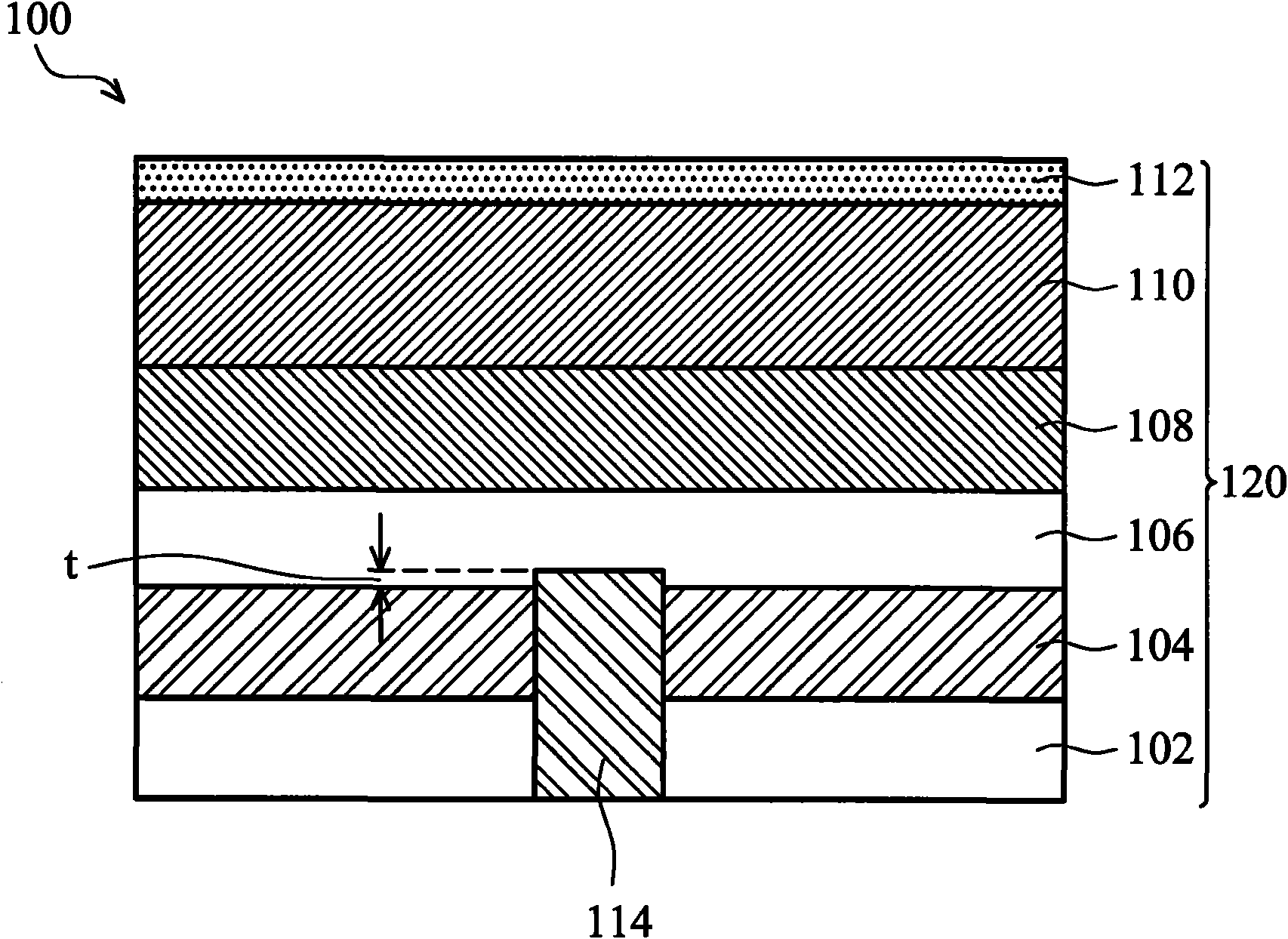
[0016] figure 1 A first embodiment of an LED of the present invention is shown, comprising a patterned substrate containing a mosaic bottom electrode. The LED 100 includes a substrate 102 and an LED structure 120 formed on the substrate 102 . The substrate 102 may include a conductive substrate or a non-conductive substrate. Non-conductive substrates can be sapphire, MgAl 2 o 4 , single crystal oxide or the like. The semiconductor substrate may be GaN, Si, Ge, SiC, SiGe, ZnO, ZnS, ZnSe, GaP, GaAs or the like. The substrate 102 may have a thickness of about 200 μm to about 600 μm. Epitaxial film formed LED structure 120 grown on substrate 102, which includes buffer / nucleation layer 104, first contact III-nitride layer 106, active layer 108, second contact III-nitride layer 110, and top contact layer 112 .

[0017] The buffer / nucleation layer 104 can be a low temperature or high temperature grown III-nitride layer, III-nitride superlattice layer, metal carbon-nitrogen lay...


PUM


Abstract

A light emitting diode (LED) device is presented. The LED device includes a substrate, a layered LED structure, and an embedded bottom electrode. The layered LED structure includes a buffer / nucleation layer disposed on the substrate, an active layer, and a top-side contact. A first-contact III-nitride layer is interposed between the buffer / nucleation layer and the active layer. A second-contact III-nitride layer is interposed between the active well layer and the top-side contact. A bottom electrode extends through the substrate, through the buffer / nucleation layer and terminates within the first-contact III-nitride layer.

Description

technical field [0001] The present invention relates to a light emitting diode (LED), and more particularly to a vertical Ill-nitride LED disposed on a patterned substrate with a mosaic bottom electrode. Background technique [0002] The manufacture of light-emitting diodes (LEDs) is mainly formed by forming an active region on the substrate, various conductors and semiconductors on the substrate, which utilizes the radiative combination of electrons and holes to generate current at the p-n junction and emit electromagnetic radiation. Electromagnetic radiation can be generated by direct bandgap materials, such as GaAs or GaN, creating a forward bias of the p-n junction and introducing electrons and holes to combine into the depletion region. Electromagnetic radiation can be visible or invisible. Different bandgap materials can produce LEDs of different colors. In addition, the invisible light excited by the LED can directly irradiate the phosphor or the like, and the phosp...

Claims


Application Information

Patent Timeline
Patent Type & Authority Applications(China)
IPC IPC(8): H01L33/00
CPCH01L33/14H01L33/20H01L33/0079H01L33/007H01L33/38H01L33/382H01L2933/0016H01L33/0093
Inventor 余振华余佳霖邱文智陈鼎元林宏达
Owner TAIWAN SEMICON MFG CO LTD
Why Eureka
Try Eureka