In2Te3 phase-change memory element and preparation method thereof

A technology of phase change memory and components, which is applied to electrical components, ion implantation plating, coatings, etc., can solve the problems of inability to achieve fast reading and writing, difficulty in further improving recording density, etc., achieve excellent switching characteristics, improve component structure, The effect of significant difference in resistance value

Inactive Publication Date: 2009-12-30
NANJING UNIV
View PDF0 Cites 2 Cited by
  • Summary
  • Abstract
  • Description
  • Claims
  • Application Information

AI Technical Summary

Problems solved by technology

However, the currently used non-volatile magnetic media memory cannot achieve fast reading and writing due to the mechanical movement of the magnetic head and the recording medium during the reading and writing process, and it is difficult to further increase the recording density.

Method used


Image

  • In2Te3 phase-change memory element and preparation method thereof
  • In2Te3 phase-change memory element and preparation method thereof
  • In2Te3 phase-change memory element and preparation method thereof

Examples


Embodiment Construction

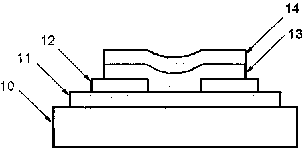
[0033] In the present invention 2 Te 3 Phase change memory element, using In 2 Te 3 The thin film is a phase-change memory storage material, and the In 2 Te 3 The film is amorphous at room temperature and becomes crystalline after annealing at 450-470°C.

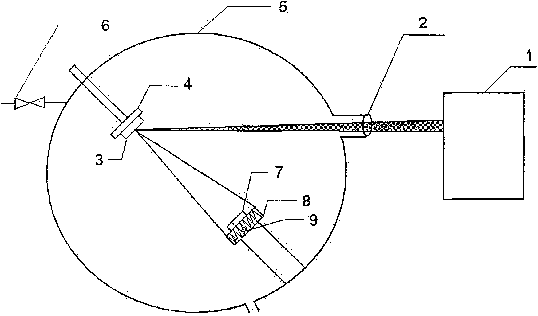
[0034] In used in the present invention 2 Te 3 The thin film is prepared by pulsed laser deposition method in the pulsed laser deposition film-making system. Firstly, In 2 Te 3 target. In 2 Te 3 The target is made by vacuum suspension melting method: a mixture of In and Te with a molar ratio of 2:3 is melted at 650-750°C, melted into a block, and then the obtained block is cut and polished into a circular target .

[0035] Afterwards, amorphous and crystalline In were prepared by pulsed laser deposition film forming system. 2 Te 3 film materials such as figure 2 :

[0036] a) put In 2 Te 3 The alloy target 3 is fixed on the target stage 4 of the pulsed laser deposition film-making system, the substrate 7 i...


PUM

PropertyMeasurementUnit
Thicknessaaaaaaaaaa
Apertureaaaaaaaaaa

Abstract

The invention relates to an In2Te3 phase-change memory element and a preparation method thereof. The In2Te3 phase-change memory element is characterized in that an In2Te3 membrane is adopted as phase-change memory storage material, wherein the In2Te3 membrane is in an amorphous state at room temperature and is in a crystalline state after anneal at 450-470 DEG C, the basic configuration of the phase-change memory element is of a three-layer structure which is formed in such a way that one layer of In2Te3 membrane is clamped between a top electrode film and a bottom electrode film, and the top electrode film and the bottom electrode film respectively lead out wire leads made of spun gold or brass wires. The invention realizes the switching effect in tests and has the characteristics that the differences of resistance values of the In2Te3 membrane in an amorphous state and in a crystalline state are obvious and can reach 3-4 orders of magnitude; the phase-change speed / read-write speed is fast, the working volt is low, and the needed voltage pulse achieves ns magnitudes; and a plurality of circular changes can be made between a high-impedance state and a low-impedance state.

Description

technical field [0001] The invention belongs to the field of microelectronic devices and materials thereof, and in particular relates to a novel fast read-write high-density In-based 2 Te 3 Amorphous and crystalline phase change memory elements of thin film materials and In 2 Te 3 The preparation method of film material is a kind of In 2 Te 3 Phase-change memory element and its preparation method. Background technique [0002] For nearly half a century, the development of integrated circuits has basically followed the prediction made by G.E. Moore: "The number of components integrated on a single chip doubles every eighteen months." With the continuous development of semiconductor technology and the integration of more and more electronic devices into people's work and life, traditional devices can no longer meet people's basic needs. Therefore, the development of new storage technologies and devices with high density, low energy consumption, and high-speed repeated re...

Claims


Application Information

Patent Timeline
IPC IPC(8): H01L45/00C23C14/28C23C14/14C23C14/35C23C14/10
Inventor 殷江朱颢夏奕东刘治国
Owner NANJING UNIV
Why Eureka
Try Eureka