Conducting wire stack type suture joint in semiconductor device

A technology of semiconductors and sutures, which is applied in the field of low-profile semiconductor devices and its manufacturing, can solve the problems of high suture failure rate, bulky structure, and increase of manufacturing process steps and time, and achieve low suture rupture rate and few steps , the effect of less production time

Inactive Publication Date: 2009-12-30
SANDISK CORP
View PDF5 Cites 1 Cited by
  • Summary
  • Abstract
  • Description
  • Claims
  • Application Information

AI Technical Summary

Problems solved by technology

First, having to add extra stitch balls in the reverse wire bonding process increases the processing steps and time of the manufacturing process, especially given the large number of bonds required in any given semiconductor package
Additionally, the ball-wire-ball configuration has a relatively bulky construction which has a high suture failure rate
In one example of a four memory die microSD package, a yield loss of about 2000PPM (parts per million) has been found

Method used


Image

  • Conducting wire stack type suture joint in semiconductor device
  • Conducting wire stack type suture joint in semiconductor device
  • Conducting wire stack type suture joint in semiconductor device

Examples


Embodiment Construction

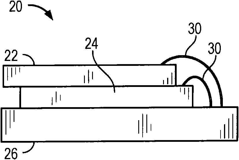
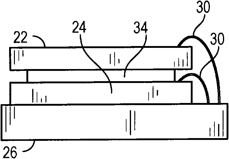
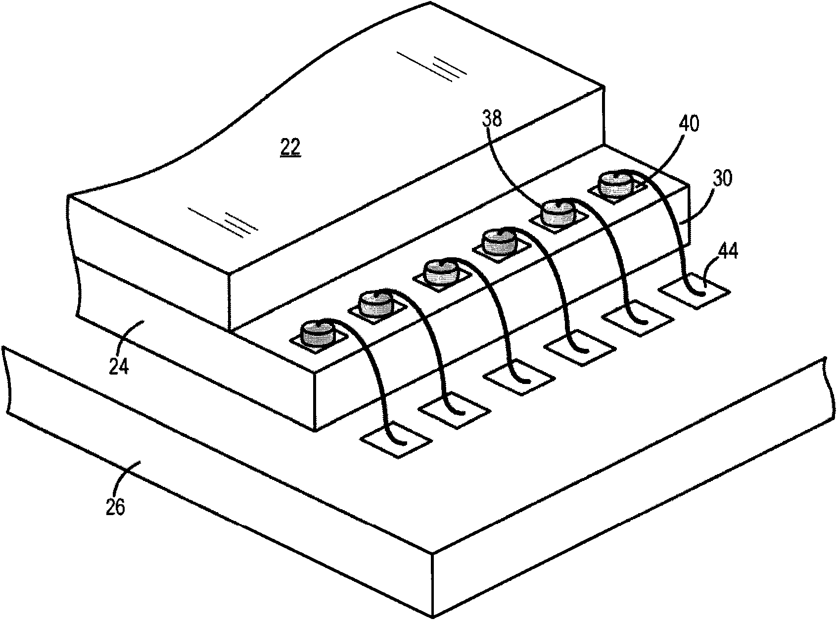
[0029] will now refer to Figure 6 to Figure 12 Embodiments will be described, which relate to low-profile semiconductor packages. It should be understood that the invention may be embodied in many different forms and should not be construed as limited to the embodiments set forth herein. Rather, these embodiments are provided so that this disclosure will be thorough and complete, and will fully convey the invention to those skilled in the art. Indeed, the invention is intended to cover alternatives, modifications and equivalents of these embodiments, which are included within the scope and spirit of the invention as defined by the appended claims. Furthermore, in the following detailed description of the invention, numerous specific details are set forth in order to provide a thorough understanding of the invention. It will be apparent, however, to one of ordinary skill in the art that the present invention may be practiced without such specific details.

[0030] The terms...


PUM


Abstract

The invention discloses low-profile semiconductor package comprising at least a first stacking semiconductor circuit small piece and a second stacking semiconductor circuit small piece which are arranged on a substrate, wherein the first semiconductor circuit small piece can be electrically coupled to the substrate by a plurality of sutures in a forward pillow joint technology, the second semiconductor circuit small piece can be electrically coupled to the first semiconductor circuit small piece by a second group of sutures which are jointed between circuit small piece joint pads of the first semiconductor circuit small piece and the second semiconductor circuit small piece, each suture of the second group of sutures comprises a suture ball, the front end of the suture ball is connected to the joint pad of the second semiconductor circuit small piece, and the tail end of each suture of the second group of sutures can be directly connected to the front end of the suture of a first group of sutures in a wedge shape.

Description

technical field [0001] Embodiments of the present invention relate to a low-profile semiconductor device and a method of manufacturing the same. Background technique [0002] The strong growth in demand for portable consumer electronics is driving the need for high capacity storage devices. Non-volatile semiconductor memory devices, such as flash memory memory cards, are becoming widely used to meet the ever-increasing demand for digital information storage and exchange. Its portability, versatility and rugged design, as well as its high reliability and large capacity make such memory devices ideal for use in a variety of electronic devices including, for example, digital cameras, digital music players, video games Consoles, PDAs and cellular phones. [0003] Although a variety of packaging configurations are known, flash memory memory cards are typically manufactured as system-in-a-package (SiP) or multi-chip modules (MCM), where functional systems are assembled into a si...

Claims


Application Information

Patent Timeline
Patent Type & Authority Applications(China)
IPC IPC(8): H01L21/60H01L25/00H01L25/065H01L25/18H01L23/49
CPCH01L2224/85205H01L2224/48479H01L2224/45124H01L2224/45H01L2224/4911H01L2924/01082H01L2924/00014H01L2224/97H01L2224/48699H01L24/85H01L2924/01019H01L2924/01322H01L2224/85045H01L2924/01029H01L2225/06555H01L2224/85951H01L2224/48147H01L2224/48091H01L2924/01013H01L24/49H01L2224/85051H01L2224/45147H01L24/97H01L24/48H01L24/45H01L2224/48599H01L2224/4845H01L2224/4554H01L2924/1433H01L2224/48145H01L2924/01079H01L2224/4569H01L2224/48465H01L25/0657H01L2224/48227H01L2924/14H01L2924/01033H01L2924/01005H01L2224/32145H01L2924/01006H01L2225/0651H01L2924/01078H01L2224/85986H01L2224/48471H01L2224/45144H01L2225/06562H01L2224/48799H01L2225/06506H01L2924/181H01L2224/05554H01L2224/05553H01L2224/48644H01L2224/48744H01L2224/48844H01L2224/49175H01L2224/49429H01L2224/85181H01L2224/85444H01L2224/85186H01L2224/85H01L2224/78H01L2924/00H01L2224/45099H01L2924/00015H01L2924/00012H01L23/12H01L23/49H01L25/065
Inventor 梁行志方海波王丽
Owner SANDISK CORP
Why Eureka
Try Eureka